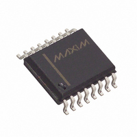
MAX532BCWE+T Maxim Integrated Products, MAX532BCWE+T Datasheet - Page 4

MAX532BCWE+T
Manufacturer Part Number
MAX532BCWE+T
Description
IC MDAC 12BIT DUAL SER 16-SOIC
Manufacturer
Maxim Integrated Products
Datasheet
1.MAX532ACPE.pdf
(16 pages)
Specifications of MAX532BCWE+T
Settling Time
2.5µs
Number Of Bits
12
Data Interface
Serial
Number Of Converters
2
Voltage Supply Source
Dual ±
Power Dissipation (max)
762mW
Operating Temperature
0°C ~ 70°C
Mounting Type
Surface Mount
Package / Case
16-SOIC (0.300", 7.5mm Width)
Lead Free Status / RoHS Status
Lead free / RoHS Compliant
TIMING CHARACTERISTICS
(V
Dual, Serial-Input,
Voltage-Output, 12-Bit MDAC
ELECTRICAL CHARACTERISTICS (continued)
(V
VOUT_ connected to RFB_, T
Note 1: Static performance tested at V
Note 2: Guaranteed by design. Not subject to production testing.
Note 3: Open-drain output.
Note 4: All input signals are specified with t
Note 5: See Figure 1.
Note 6: Timing is for SCLK fall to DOUT fall to 0.8V, or for SCLK fall to DOUT rise to 2.4V. Additional time must be added for any
Note 7: DOUT enable: DOUT falls to 4.5V from 5.0V. DOUT disable: DOUT rises to 0.5V from 0V.
4
Multiplying Feedthrough
Error
Unity-Gain Small-Signal
Bandwidth
Full-Power Bandwidth
Total Harmonic Distortion
Digital Feedthrough
Digital Crosstalk
Output Noise Voltage
SCLK Clock Frequency
SCLK Pulse Width High
SCLK Pulse Width Low
DIN to SCLK Rise Setup Time
DIN to SCLK Rise Hold Time
CS Fall to SCLK Rise Setup Time
CS Rise to SCLK Rise Setup Time
SCLK Fall to CS Fall Hold Time
SCLK Rise to CS Rise Hold Time
CS Pulse Width High
SCLK Fall to DOUT Valid (Note 6)
CS Fall to DOUT Enable (Note 7)
CS Rise to DOUT Disable (Note 7)
LDAC Pulse Width Low
CS Rise to LDAC Fall Setup Time
DD
DD
_______________________________________________________________________________________
= 11.4V to 16.5V, V
= 11.4V to 16.5V, V
PARAMETER
larger passive RC pull-up delay.
PARAMETER
SS
SS
= -11.4V to -16.5V, AGNDA = AGNDB = DGND = 0V) (Notes 4, 5)
= -11.4V to -16.5V, AGNDA = AGNDB = DGND = 0V, VREFA and VREFB = +10V, R
SYMBOL
A
= T
THD
MIN
to T
DD
VREF = 20V
DAC latch loaded with all 0s
VREF = 100mV
DAC latch loaded with all 1s
VREF = 20V
DAC latch loaded with all 1s
VREF = 6V
DAC latch loaded with all 1s
CS = 1; transitions on SCLK, LDAC, DIN
DACA code all 1s, DACB code transition from all 0s to all 1s
0.1Hz to 10Hz
SYMBOL
MAX
= +15V, V
t
t
t
t
t
t
LDACS
t
CSH0
CSH1
LDAC
f
CSS0
CSS1
R
t
t
CSW
t
CLK
t
t
t
t
CH
DS
DH
DO
DV
, unless otherwise noted.)
CL
TR
= t
F
RMS
5ns. Logic input swing is 0V to 5V.
SS
p-p
p-p
C
C
C
L
L
L
= -15V. Performance over supplies guaranteed by PSR test.
, 1kHz sine wave;
p-p
= 20pF, R
= 20pF, R
= 20pF, R
10kHz sine wave;
sine wave;
sine wave;
CONDITIONS
PULL-UP
PULL-UP
PULL-UP
CONDITIONS
= 1kΩ to 5V
= 1kΩ to 5V
= 1kΩ to 5V
MIN
MIN
80
80
50
0
50
50
5
80
120
0
60
100
TYP
TYP
125
-77
1.0
-90
1.1
10
2
L
= 2kΩ, C
MAX
MAX
6.25
200
100
60
L
= 100pF,
UNITS
µV
UNITS
MHz
nV-s
nV-s
MHz
kHz
dB
dB
ns
ns
ns
ns
ns
ns
ns
ns
ns
ns
ns
ns
ns
ns
RMS


