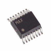
MAX5156AEEE+T Maxim Integrated Products, MAX5156AEEE+T Datasheet - Page 3

MAX5156AEEE+T
Manufacturer Part Number
MAX5156AEEE+T
Description
IC DAC 12BIT DUAL LP SER 16-QSOP
Manufacturer
Maxim Integrated Products
Datasheet
1.MAX5156BCEE.pdf
(16 pages)
Specifications of MAX5156AEEE+T
Settling Time
15µs
Number Of Bits
12
Data Interface
Serial
Number Of Converters
2
Voltage Supply Source
Single Supply
Power Dissipation (max)
667mW
Operating Temperature
-40°C ~ 85°C
Mounting Type
Surface Mount
Package / Case
16-QSOP
Lead Free Status / RoHS Status
Lead free / RoHS Compliant
ELECTRICAL CHARACTERISTICS—MAX5156 (continued)
(V
T
Note 1: Accuracy is specified from code 10 to code 4095.
Note 2: Accuracy is better than 1LSB for V
Note 3: Digital inputs are set to either V
Note 4: SCLK minimum clock period includes rise and fall times.
DIGITAL OUTPUTS (DOUT, UPO)
Output High Voltage
Output Low Voltage
DYNAMIC PERFORMANCE
Voltage Output Slew Rate
Output Settling Time
Output Voltage Swing
Current into FBA or FBB
Time Required to Exit Shutdown
Digital Feedthrough
Digital Crosstalk
POWER SUPPLIES
Positive Supply Voltage
Power-Supply Current
Power-Supply Current in
Shutdown
Reference Current in Shutdown
TIMING CHARACTERISTICS
SCLK Clock Period
SCLK Pulse Width High
SCLK Pulse Width Low
CS Fall to SCLK Rise Setup Time
SCLK Rise to CS Rise Hold Time
DIN Setup Time
DIN Hold Time
SCLK Rise to DOUT Valid
Propagation Delay
SCLK Fall to DOUT Valid
Propagation Delay
SCLK Rise to CS Fall Delay
CS Rise to SCLK Rise Hold
CS Pulse Width High
A
DD
= +25°C, output buffer connected in unity-gain configuration (Figure 9).)
= +5V ±10%, V
Low-Power, Dual, 12-Bit Voltage-Output DACs
PARAMETER
REFA
_______________________________________________________________________________________
= V
REFB
I
SYMBOL
= 2.5V, R
DD(SHDN)
t
t
t
t
V
t
t
t
V
V
CSW
I
t
CHS
t
DO1
DO2
I
t
t
CSS
t
CS0
CS1
SR
DD
CH
DH
FB
CP
CL
DS
OH
DD
OL
DD
OUT
or DGND, code = 0000 hex, R
L
= 10kΩ, C
greater than 6mV and less than V
I
I
To 1/2LSB of full-scale, V
Rail-to-rail (Note 2)
CS = V
(Note 3)
(Note 3)
(Note 4)
C
C
SOURCE
SINK
LOAD
LOAD
= 2mA
DD
= 200pF
= 200pF
= 2mA
L
, f
= 100pF, T
DIN
with Configurable Outputs
CONDITIONS
= 100kHz, V
A
= T
STEP
L
MIN
SCLK
=
= 2.5V
DD
to T
.
= 5Vp-p
- 50mV. Guaranteed by PSRR test at the end points.
MAX
, unless otherwise noted. Typical values are at
V
DD
MIN
100
100
4.5
40
40
40
40
10
40
0
0
- 0.5
0 to V
TYP
0.13
0.75
0.5
15
25
0
5
5
2
0
DD
MAX
±0.1
0.40
0.65
5.5
±1
10
80
80
UNITS
V/µs
nV-s
nV-s
mA
µA
µA
µA
µs
µs
ns
ns
ns
ns
ns
ns
ns
ns
ns
ns
ns
ns
V
V
V
V
3


