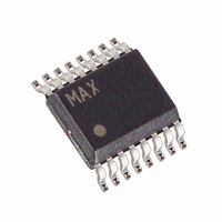
MAX5156AEEE+T Maxim Integrated Products, MAX5156AEEE+T Datasheet - Page 9

MAX5156AEEE+T
Manufacturer Part Number
MAX5156AEEE+T
Description
IC DAC 12BIT DUAL LP SER 16-QSOP
Manufacturer
Maxim Integrated Products
Datasheet
1.MAX5156BCEE.pdf
(16 pages)
Specifications of MAX5156AEEE+T
Settling Time
15µs
Number Of Bits
12
Data Interface
Serial
Number Of Converters
2
Voltage Supply Source
Single Supply
Power Dissipation (max)
667mW
Operating Temperature
-40°C ~ 85°C
Mounting Type
Surface Mount
Package / Case
16-QSOP
Lead Free Status / RoHS Status
Lead free / RoHS Compliant
The MAX5156/MAX5157 dual, 12-bit, voltage-output
DACs are easily configured with a 3-wire serial inter-
face. These devices include a 16-bit data-in/data-out
shift register, and each DAC has a double-buffered
input comprised of an input register and a DAC register
(see Functional Diagram ). Both DACs use an inverted
R-2R ladder network that produces a weighted voltage
proportional to the input voltage value. Each DAC has
its own reference input to facilitate independent full-
scale values. Figure 1 depicts a simplified circuit dia-
gram of one of the two DACs.
The reference inputs accept both AC and DC values
with a voltage range extending from 0V to (V
Determine the output voltage using the following equa-
tion:
where NB is the numeric value of the DAC’s binary input
code (0 to 4095) and V
The reference input impedance ranges from 14kΩ (1554
hex) to several giga ohms (with an input code of 0000
hex). This reference input capacitance is code depen-
dent and typically ranges from 15pF with an input code
of all zeros to 50pF with a full-scale input code.
_______________Detailed Description
______________________________________________________________Pin Description
PIN
10
11
12
13
14
15
16
1
2
3
4
5
6
7
8
9
Low-Power, Dual, 12-Bit Voltage-Output DACs
NAME
AGND
DGND
DOUT
OUTA
OUTB
REFA
SCLK
REFB
UPO
FBA
PDL
FBB
V
DIN
CL
CS
DD
V
OUT
_______________________________________________________________________________________
= V
Analog Ground
DAC A Output Voltage
DAC A Output Amplifier Feedback Input. Inverting input of the output amplifier.
Reference for DAC A
Active-Low Clear Input. Resets all registers to zero. DAC outputs go to 0V.
Chip-Select Input
Serial Data Input
Serial Clock Input
Digital Ground
Serial Data Output
User-Programmable Output
Power-Down Lockout. The device cannot be powered down when PDL is low.
Reference Input for DAC B
DAC B Output Amplifier Feedback Input. Inverting input of the output amplifier.
DAC B Output Voltage
Positive Power Supply
REF
REF
is the reference voltage.
x NB / 4096
Reference Inputs
DD
- 1.4V).
with Configurable Outputs
The output amplifier’s inverting input is available to the
user, allowing force and sense capability for remote
sensing and specific gain configurations. The inverting
input can be connected to the output to provide a unity-
gain buffered output. The output amplifiers have a typi-
cal slew rate of 0.75V/µs and settle to 1/2LSB within
15µs, with a load of 10kΩ in parallel to 100pF. Loads
less than 2kΩ degrade performance.
Figure 1. Simplified DAC Circuit Diagram
AGND
FUNCTION
REF_
SHOWN FOR ALL 1s ON DAC
2R
2R
D0
R
2R
D9
R
2R
D10
R
Output Amplifier
2R
D11
FB_
OUT_
9


