MAX5856AECM+TD Maxim Integrated Products, MAX5856AECM+TD Datasheet - Page 22
MAX5856AECM+TD
Manufacturer Part Number
MAX5856AECM+TD
Description
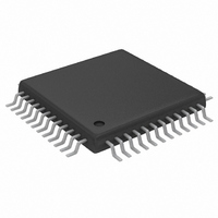
IC DAC 8BIT DUAL 300MSPS 48-TQFP
Manufacturer
Maxim Integrated Products
Datasheet
1.MAX5856AECMD.pdf
(23 pages)
Specifications of MAX5856AECM+TD
Settling Time
11ns
Number Of Bits
8
Data Interface
Parallel
Number Of Converters
2
Voltage Supply Source
Single Supply
Power Dissipation (max)
792mW
Operating Temperature
-40°C ~ 85°C
Mounting Type
Surface Mount
Package / Case
48-TQFP Exposed Pad, 48-eTQFP, 48-HTQFP, 48-VQFP
Lead Free Status / RoHS Status
Lead free / RoHS Compliant


The MAX5856A is packaged in a 48-pin TQFP-EP
package, providing design flexibility, increased thermal
efficiency, and optimized AC performance of the DAC.
The EP enables the implementation of grounding tech-
niques necessary to ensure highest performance.
In this package, the data converter die is attached to
an EP lead frame with the back of this frame exposed
at the package bottom surface, facing the PC board
side of the package. This allows a solid attachment of
the package to the PC board with standard infrared
(IR)-flow soldering techniques. A specially created land
pattern on the PC board, matching the size of the EP,
ensures the proper attachment and grounding of the
DAC. Designing vias into the land area and implement-
ing large ground planes in the PC board design
achieve optimal DAC performance. Use an array of 3 x
3 (or greater) vias (≤0.3mm diameter per via hole and
1.2mm pitch between via holes) for this 48-pin TQFP-
EP package.
THD is the ratio of the RMS sum of all essential harmon-
ics (within a Nyquist window) of the input signal to the
fundamental itself. This can be expressed as:
where V 1 is the fundamental amplitude, and V 2 through
V N are the amplitudes of the 2nd through Nth order
harmonics.
SFDR is the ratio of RMS amplitude of the carrier fre-
quency (maximum signal component) to the RMS value
of the next-largest spectral component. SFDR is usually
measured in dBc with respect to the carrier frequency
amplitude or in dBFS with respect to the DAC’s full-
scale range. Depending on its test condition, SFDR is
observed within a predefined window or to Nyquist.
A series of equally spaced tones are applied to the
DAC with one tone removed from the center of the
range. MTPR is defined as the worst-case distortion
(usually a 3rd-order harmonic product of the fundamen-
tal frequencies), which appears as the largest spur at
the frequency of the missing tone in the sequence. This
test can be performed with any number of input tones;
however, four and eight tones are among the most
Dual 8-Bit, 300Msps DAC with 4x/2x/1x
Interpolation Filters and PLL
22
THD
______________________________________________________________________________________
Spurious-Free Dynamic Range (SFDR)
=
20
Total Harmonic Distortion (THD)
×
log
Multitone Power Ratio (MTPR)
Dynamic Performance
Parameter Definitions
(
V
2
2
+
V
3
2
+
V
4
2
... ...
+
V
N
2
)
/
V
1
common test conditions for CDMA- and GSM/EDGE-
type applications.
The two-tone IMD is the ratio expressed in dBc of either
output tone to the worst 3rd-order (or higher) IMD prod-
ucts.
Integral nonlinearity (INL) is the deviation of the values
on an actual transfer function from a line drawn
between the end points of the transfer function, once
offset and gain errors have been nullified. For a DAC,
the deviations are measured at every individual step.
Differential nonlinearity (DNL) is the difference between
an actual step height and the ideal value of 1 LSB. A
DNL error specification ≥ -1 LSB guarantees a monoto-
nic transfer function.
Offset error is the current flowing from positive DAC
output when the digital input code is set to zero. Offset
error is expressed in LSBs.
A gain error is the difference between the ideal and the
actual full-scale output current on the transfer curve,
after nullifying the offset error. This error alters the slope
of the transfer function and corresponds to the same
percentage error in each step. The ideal current is
defined by reference voltage at V
The settling time is the amount of time required from the
start of a transition until the DAC output settles to its new
output value (within the converter’s specified accuracy).
A glitch is generated when a DAC switches between
two codes. The largest glitch is usually generated
around the midscale transition, when the input pattern
transitions from 011…111 to 100…000. This occurs due
to timing variations between the bits. The glitch impulse
is found by integrating the voltage of the glitch at the
midscale transition over time. The glitch impulse is usu-
ally specified in pV-s.
TRANSISTOR COUNT: 178,376
PROCESS: CMOS
Static Performance Parameter Definitions
Intermodulation Distortion (IMD)
Differential Nonlinearity (DNL)
Integral Nonlinearity (INL)
Chip Information
REFO
/ I
Glitch Impulse
REF
Settling Time
Offset Error
Gain Error
x 32.
Related parts for MAX5856AECM+TD
Image
Part Number
Description
Manufacturer
Datasheet
Request
R

Part Number:
Description:
MAX7528KCWPMaxim Integrated Products [CMOS Dual 8-Bit Buffered Multiplying DACs]
Manufacturer:
Maxim Integrated Products
Datasheet:
Part Number:
Description:
Single +5V, fully integrated, 1.25Gbps laser diode driver.
Manufacturer:
Maxim Integrated Products
Datasheet:
Part Number:
Description:
Single +5V, fully integrated, 155Mbps laser diode driver.
Manufacturer:
Maxim Integrated Products
Datasheet:
Part Number:
Description:
VRD11/VRD10, K8 Rev F 2/3/4-Phase PWM Controllers with Integrated Dual MOSFET Drivers
Manufacturer:
Maxim Integrated Products
Datasheet:
Part Number:
Description:
Highly Integrated Level 2 SMBus Battery Chargers
Manufacturer:
Maxim Integrated Products
Datasheet:
Part Number:
Description:
Current Monitor and Accumulator with Integrated Sense Resistor; ; Temperature Range: -40°C to +85°C
Manufacturer:
Maxim Integrated Products
Part Number:
Description:
TSSOP 14/A�/RS-485 Transceivers with Integrated 100O/120O Termination Resis
Manufacturer:
Maxim Integrated Products
Part Number:
Description:
TSSOP 14/A�/RS-485 Transceivers with Integrated 100O/120O Termination Resis
Manufacturer:
Maxim Integrated Products
Part Number:
Description:
QFN 16/A�/AC-DC and DC-DC Peak-Current-Mode Converters with Integrated Step
Manufacturer:
Maxim Integrated Products
Part Number:
Description:
TDFN/A/65V, 1A, 600KHZ, SYNCHRONOUS STEP-DOWN REGULATOR WITH INTEGRATED SWI
Manufacturer:
Maxim Integrated Products
Part Number:
Description:
Integrated Temperature Controller f
Manufacturer:
Maxim Integrated Products
Part Number:
Description:
SOT23-6/I�/45MHz to 650MHz, Integrated IF VCOs with Differential Output
Manufacturer:
Maxim Integrated Products
Part Number:
Description:
SOT23-6/I�/45MHz to 650MHz, Integrated IF VCOs with Differential Output
Manufacturer:
Maxim Integrated Products
Part Number:
Description:
EVALUATION KIT/2.4GHZ TO 2.5GHZ 802.11G/B RF TRANSCEIVER WITH INTEGRATED PA
Manufacturer:
Maxim Integrated Products
Part Number:
Description:
QFN/E/DUAL PCIE/SATA HIGH SPEED SWITCH WITH INTEGRATED BIAS RESISTOR
Manufacturer:
Maxim Integrated Products
Datasheet: