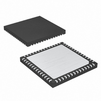
MAX5733AUTN+ Maxim Integrated Products, MAX5733AUTN+ Datasheet - Page 16

MAX5733AUTN+
Manufacturer Part Number
MAX5733AUTN+
Description
IC DAC 16BIT 32CHAN SER 56-TQFN
Manufacturer
Maxim Integrated Products
Datasheet
1.MAX5732BUTNT.pdf
(28 pages)
Specifications of MAX5733AUTN+
Settling Time
20µs
Number Of Bits
16
Data Interface
MICROWIRE™, QSPI™, Serial, SPI™
Number Of Converters
32
Voltage Supply Source
Analog and Digital
Power Dissipation (max)
2.5W
Operating Temperature
0°C ~ 85°C
Mounting Type
Surface Mount
Package / Case
56-TQFN
Lead Free Status / RoHS Status
Lead free / RoHS Compliant
32-Channel, 16-Bit, Voltage-Output
DACs with Serial Interface
The MAX5732–MAX5735 are 32-channel, 16-bit, volt-
age-output DACs (Figure 1). The devices accept a 3V
external reference input at REF. An internal offset DAC
allows all outputs to be offset (see Table 1). The devices
provide a ground-sensing function that allows the output
voltages to be referenced to a remote ground.
A 33MHz SPI-/QSPI/-MICROWIRE- and DSP-compatible
serial interface controls the MAX5732–MAX5735 (Figure 2).
Each DAC includes a double-buffered input structure to
minimize the digital noise feedthrough from the digital
inputs to the outputs, and allows for synchronous or
asynchronous updating of the outputs. The two buffers
are organized as an input register followed by a DAC
register that stores the contents of the output. Input reg-
isters update the DAC registers independently or simul-
taneously with a single software or hardware command.
The MAX5732–MAX5735 also have a DOUT that allows
for read-back or daisy chaining multiple devices.
The MAX5732–MAX5735 analog and digital sections
have separate power inputs. Separate power inputs are
also provided for the output buffer amplifiers.
Proprietary deglitch circuits prevent output glitches at
power-up and eliminate the need for power sequenc-
ing. A software-shutdown mode allows efficient power
management. The MAX5732–MAX5735 consume 50µA
of supply current in shutdown.
All DACs provide buffered outputs that can drive 10kΩ
in parallel with 100pF. The MAX5732 has a 0 to +5V
output range; the MAX5733 has a 0 to +10V output
Figure 2. Serial-interface Timing
16
(DSP MODE)
(µC MODE)
______________________________________________________________________________________
SCLK
DIN
CS
CS
X
t
SCS
Detailed Description
t
CSPWH
X
t
CSPWL
t
CSS
1
t
DS
C2
t
DH
2
C1
t
CL
range; the MAX5734 has a -2.5V to +7.5V output range;
and the MAX5735 has a -5V to +5V output range.
The REF voltage sets the full-scale output voltage for all
32 DACs. REF accepts a +3V ±3% input. Reference
voltages outside these limits can result in a degradation
of device performance.
REF is a buffered input. The typical input impedance is
10MΩ, and it does not vary with code. Use a high-
accuracy, low-noise voltage reference such as the
MAX6126AASA30 (3ppm/°C temp drift and 0.02% initial
accuracy) to improve static accuracy. REF does not
accept AC signals.
The MAX5732–MAX5735 include a GS that allows the
output voltages to be referenced to a remote ground.
The GS input voltage range (V
V
resulting output voltage must be within the valid output-
voltage range set by the power supplies. See the
Output Amplifiers (OUT0–OUT31) section for the effect
of the GS inputs on the DAC outputs.
The MAX5732–MAX5735 feature an offset DAC that
determines the output voltage range. While each part
number has an output voltage range associated with it,
it is the offset DAC that determines the end-point volt-
ages of the range. Table 1 shows the offset DAC code
required during power-up.
GS
t
CH
3
is added to the output voltage with unity gain. The
C0
External Reference Input (REF)
32
D0
t
CS2
Ground Sense (GS)
GS
) is -0.5V to +0.5V.
t
CS1
Offset DAC
X


