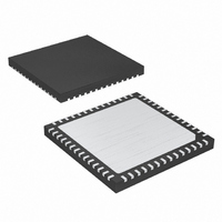
MAX5732AUTN+ Maxim Integrated Products, MAX5732AUTN+ Datasheet - Page 25

MAX5732AUTN+
Manufacturer Part Number
MAX5732AUTN+
Description
IC DAC 16BIT 32CHAN SER 56-TQFN
Manufacturer
Maxim Integrated Products
Datasheet
1.MAX5732BUTNT.pdf
(28 pages)
Specifications of MAX5732AUTN+
Settling Time
20µs
Number Of Bits
16
Data Interface
MICROWIRE™, QSPI™, Serial, SPI™
Number Of Converters
32
Voltage Supply Source
Analog and Digital
Power Dissipation (max)
2.5W
Operating Temperature
0°C ~ 85°C
Mounting Type
Surface Mount
Package / Case
56-TQFN
Lead Free Status / RoHS Status
Lead free / RoHS Compliant
protection on their reference inputs to satisfy absolute
maximum ratings. The MAX5734 features outputs that
are almost rail-to-rail. This allows the AV
supplies to be set to voltages within the absolute maxi-
mum ratings of the PEIC. This guarantees that the PEIC
is protected in all situations.
Additional protection is provided by the MAX5734
glitch-free power-up into the clear state with all DAC
outputs set to approximately 0V. Either the serial port or
the CLR input can assert the clear function.
Grounding and power-supply decoupling strongly influ-
ence device performance. Digital signals can couple
through the reference input, power supplies, and ground
connection. Proper grounding and layout can reduce
AGND
OUT9
OUT8
OUT7
OUT6
OUT5
OUT4
OUT3
OUT2
OUT1
OUT0
AV
N.C.
N.C.
N.C.
V
CC
SS
TOP VIEW
10
12
13
14
15
16
11
Pin Configurations (continued)
1
2
3
4
5
6
7
8
9
64
17
63
18
62
19
61
20
______________________________________________________________________________________
60
21
Power Supplies, Bypassing,
59
22
MAX5732–MAX5735
58
23
Decoupling, and Layout
TQFP
57
24
56
25
55
26
32-Channel, 16-Bit, Voltage-Output
54
27
53
28
52
29
51
30
50
31
CC
49
32
and V
48
47
46
45
44
43
42
41
40
38
37
36
35
34
33
39
AV
OUT21
OUT22
V
AGND
OUT23
OUT24
OUT25
OUT26
OUT27
OUT28
OUT29
OUT30
OUT31
N.C.
N.C.
SS
CC
DACs with Serial Interface
SS
digital feedthrough and crosstalk. Bypass all power sup-
plies with an additional 0.1µF and 1µF on each pin, as
close to the device as possible. Refer to the MAX5732–
MAX5735 evaluation kit for a suggested layout.
The MAX5732–MAX5735 have four separate power
supplies. AV
(except for the output buffers) and DV
digital section of the device. AV
output buffers.
The MAX5732–MAX5735 feature an exposed paddle on
the backside of the package for improved power dissi-
pation. The exposed paddle is electrically connected to
V
that shares the same potential. For more information on
the exposed paddle QFN package, refer to the following
website: http://pdfserv.maxim-ic.com/arpdf/AppNotes/
4hfan081.pdf
TRANSISTOR COUNT: 152,000
PROCESS: BiCMOS
SS
, and should be soldered to a large copper plane
DD
powers the internal analog circuitry
Chip Information
CC
and V
DD
SS
powers the
power the
25


