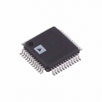
AD1953YST Analog Devices Inc, AD1953YST Datasheet - Page 27

AD1953YST
Manufacturer Part Number
AD1953YST
Description
IC DAC AUDIO 3CH 26BIT 48-LQFP
Manufacturer
Analog Devices Inc
Series
SigmaDSP®r
Datasheet
1.AD1953YSTZRL.pdf
(36 pages)
Specifications of AD1953YST
Rohs Status
RoHS non-compliant
Number Of Bits
26
Data Interface
Serial
Number Of Converters
3
Voltage Supply Source
Analog and Digital
Power Dissipation (max)
540mW
Operating Temperature
-40°C ~ 105°C
Mounting Type
Surface Mount
Package / Case
48-LQFP
For Use With
EVAL-AD1953EBZ - BOARD EVAL FOR AD1953 3CH 24BIT
Settling Time
-
Available stocks
Company
Part Number
Manufacturer
Quantity
Price
Company:
Part Number:
AD1953YSTZ
Manufacturer:
AD
Quantity:
1 450
Company:
Part Number:
AD1953YSTZ
Manufacturer:
ADI
Quantity:
455
Company:
Part Number:
AD1953YSTZ
Manufacturer:
Analog Devices Inc
Quantity:
10 000
Company:
Part Number:
AD1953YSTZRL
Manufacturer:
Analog Devices Inc
Quantity:
10 000
Company:
Part Number:
AD1953YSTZRL7
Manufacturer:
Analog Devices Inc
Quantity:
10 000
Byte 0
00000, R/Wb, Adr[9:8]
NOTES
1. ProgCount[8:0] = value of program counter where trap occurs (see Table XXI).
2. RegSel[1:0] selects one of four registers (see Data Capture Register section).
Byte 0
00000, R/Wb, Adr[9:8]
NOTES
1. ProgCount[8:0] = value of program counter where trap occurs (see Table XXI).
2. RegSel[1:0] selects one of four registers (see Data Capture Registers section).
Byte 0
00000, R/Wb, Adr[9:8] Adr[7:0]
Byte 0
00000, R/Wb, Adr[9:8] Adr[7:0]
INITIALIZATION
Power-Up Sequence
The AD1953 has a built-in power-up sequence that initializes
the contents of all internal RAMs. During this time, the contents
of the internal program boot ROM are copied to the internal
program RAM, and likewise the SPI parameter RAM is filled
with values from its associated boot ROM. The data memories
are also cleared during this time.
The boot sequence lasts for 1024 MCLK cycles and starts on
the rising edge of the RESETB pin. Since the boot sequence
requires a stable master clock, the user should avoid writing to
or reading from the SPI registers during this period of time.
Note that the default power-on state of the internal clock mode
circuitry is 512 × f
rates. This mode bypasses all the internal clock doublers and
allows the external master clock to directly operate the DSP
core. If the external master clock is 256 × f
operate at this reduced clock rate and take slightly longer to
complete. After the boot sequence has finished, the clock modes
may be set via the SPI port. For example, if the external master
clock frequency is 256 × f
take 1024 256 × f
SPI write could occur to put the AD1953 in 256 × f
The default state of the MCLK input selector is MCLK0. Since
this input selector is controlled using the SPI port, and the SPI
port cannot be written to until the boot sequence is complete,
there must be a stable master clock signal present on the MCLK0
pin at startup.
REV. 0
S
S
, or about 24 MHz for normal audio sample
Table XVII. Data_Capture_Serial Out Register (Address and Register Select) Write Format
clock cycles to complete, after which an
Byte 1
Byte 1
S
clock, the boot sequence would
Byte 1
Adr[7:0]
Byte 1
Adr[7:0]
S
, the boot sequence will
Table XVI. Data Capture Register Write Format
Byte 2
Byte 2
00000000
ParamAdr[7:0]
Table XIX. Safeload Register Write Format
Table XVIII. Data Capture Read Format
S
mode.
Byte 2
00000, ProgCount[8:6]
Byte 2
00000, ProgCount[8:6]
–27–
Byte 3
Data[23:16]
Byte 3
00, Param[21:16]
Setting the Clock Mode
The AD1953 contains a clock doubler circuit that is used to
generate an internal 512 × f
256 × f
Register 2.
When the clock mode is changed, it is possible that a glitch will
occur on the internal MCLK signal. This may cause the proces-
sor to inadvertently write an incorrect value into the data RAM,
which could cause an audio pop or click sound. To prevent this,
it is recommended that the following procedure be followed:
1. Assert the soft power-down bit (Bit <6> in Control Register 1)
2. Write the desired clock mode into Bit <2> of Control Register 2.
3. Wait at least 1 ms while the clock doublers settle.
4. Deassert the soft power-down bit.
An alternative procedure is to initiate a soft shutdown of the
processor core by writing a 1 to the halt program bit in Control
Register 1. This initiates a volume ramp-down sequence followed
by a shutdown of the DSP core. Once the core is shut down
(which can be verified by reading Bit <1> from Control Register 1,
or by waiting at least 20 ms), the new clock mode can be
programmed by writing to Bit <2> of Control Register 2. The
DSP core can then be restarted by clearing the halt program bit
in Control Register 1.
to stop the internal MCLK.
S
. The clock mode is set by writing to Bit <2> of Control
1
1
Byte 4
Data[15:8]
Byte 4
Param[15:8]
S
clock when the external clock is
Byte 3
ProgCount[5:0], RegSel[1:0]
Byte 3
ProgCount[5:0], RegSel[1:0]
AD1953
Byte 5
Data[7:0]
Byte 5
Param[7:0]
1, 2
1, 2


