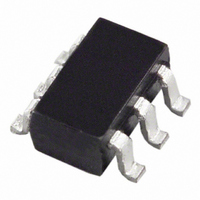
AD5301BRT-500RL7 Analog Devices Inc, AD5301BRT-500RL7 Datasheet - Page 3

AD5301BRT-500RL7
Manufacturer Part Number
AD5301BRT-500RL7
Description
IC DAC 8BIT 2WIRE I2C SOT23-6
Manufacturer
Analog Devices Inc
Datasheet
1.AD5301BRTZ-500RL7.pdf
(24 pages)
Specifications of AD5301BRT-500RL7
Rohs Status
RoHS non-compliant
Settling Time
6µs
Number Of Bits
8
Data Interface
I²C, Serial
Number Of Converters
1
Voltage Supply Source
Single Supply
Power Dissipation (max)
1.4mW
Operating Temperature
-40°C ~ 105°C
Mounting Type
Surface Mount
Package / Case
SOT-23-6
Other names
AD5301BRT-500RL7
AD5301BRT500RL7TR
AD5301BRT500RL7TR
SPECIFICATIONS
V
Table 1.
Parameter
DC PERFORMANCE
OUTPUT CHARACTERISTICS
LOGIC INPUTS (A0, A1, PD)
LOGIC INPUTS (SCL, SDA)
DD
AD5301
AD5311
AD5321
Zero-Code Error
Full-Scale Error
Gain Error
Zero-Code Error Drift
Gain Error Drift
Minimum Output Voltage
Maximum Output Voltage
DC Output Impedance
Short-Circuit Current
Power-Up Time
Input Current
Input Low Voltage, V
Input High Voltage, V
Pin Capacitance
Input High Voltage, V
Input Low Voltage, V
Input Leakage Current, I
Input Hysteresis, V
Input Capacitance, C
Glitch Rejection
= 2.5 V to 5.5 V; R
Resolution
Relative Accuracy
Differential Nonlinearity
Resolution
Relative Accuracy
Differential Nonlinearity
Resolution
Relative Accuracy
Differential Nonlinearity
2
5
6
3, 4
HYST
L
IL
IL
IN
5
IH
IH
= 2 kΩ to GND; C
5
5
IN
5
Min
2.4
2.1
2.0
0.7 × V
−0.3
0.05 × V
DD
DD
L
= 200 pF to GND; all specifications T
B Version
Typ
8
±0.15
±0.02
10
±0.5
±0.05
12
±2
±0.3
5
±0.15
±0.15
–20
−5
0.001
V
1
50
20
2.5
6
3
6
DD
− 0.001
1
Max
±1
±0.25
±4
±0.5
±16
±0.8
20
±1.25
±1
±1
0.8
0.6
0.5
V
+0.3 × V
±1
50
DD
Rev. B | Page 3 of 24
+ 0.3
DD
Unit
Bits
LSB
LSB
Bits
LSB
LSB
Bits
LSB
LSB
mV
% of FSR
% of FSR
μV/°C
ppm of FSR/°C
V
V
Ω
mA
mA
μs
μs
μA
V
V
V
V
V
V
pF
V
V
μA
V
pF
ns
MIN
to T
MAX
Conditions/Comments
Guaranteed monotonic by design over all codes.
Guaranteed monotonic by design over all codes.
Guaranteed monotonic by design over all codes.
All zeros loaded to DAC, see Figure 12.
All ones loaded to DAC, see Figure 12.
This is a measure of the minimum and maximum
drive capability of the output amplifier.
V
V
Coming out of power-down mode. V
Coming out of power-down mode. V
V
V
V
V
V
V
V
Pulse width of spike suppressed.
DD
DD
DD
DD
DD
DD
DD
DD
IN
, unless otherwise noted.
= 0 V to V
= 5 V.
= 3 V.
= 5 V ± 10%.
= 3 V ± 10%.
= 2.5 V.
= 5 V ± 10%.
= 3 V ± 10%.
= 2.5 V.
AD5301/AD5311/AD5321
DD
.
DD
DD
= 5 V.
= 3 V.


