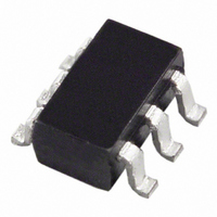
AD5301BRT-500RL7 Analog Devices Inc, AD5301BRT-500RL7 Datasheet - Page 7

AD5301BRT-500RL7
Manufacturer Part Number
AD5301BRT-500RL7
Description
IC DAC 8BIT 2WIRE I2C SOT23-6
Manufacturer
Analog Devices Inc
Datasheet
1.AD5301BRTZ-500RL7.pdf
(24 pages)
Specifications of AD5301BRT-500RL7
Rohs Status
RoHS non-compliant
Settling Time
6µs
Number Of Bits
8
Data Interface
I²C, Serial
Number Of Converters
1
Voltage Supply Source
Single Supply
Power Dissipation (max)
1.4mW
Operating Temperature
-40°C ~ 105°C
Mounting Type
Surface Mount
Package / Case
SOT-23-6
Other names
AD5301BRT-500RL7
AD5301BRT500RL7TR
AD5301BRT500RL7TR
PIN CONFIGURATIONS AND FUNCTION DESCRIPTIONS
Table 5. Pin Function Descriptions
MSOP
Pin No.
1
2
3
4
5
6
7
8
SOT-23
Pin No.
6
5
N/A
4
N/A
3
2
1
V
V
OUT
A0
A1
DD
Mnemonic
V
A0
A1
V
PD
SCL
SDA
GND
(RM-8) Pin Configuration
DD
OUT
Figure 3. 8-Lead MSOP
1
2
3
4
(Not to Scale)
AD5301/
AD5311/
TOP VIEW
AD5321
Description
Power Supply Input. These parts can be operated from 2.5 V to 5.5 V and the supply should be decoupled
with a 10 μF in parallel with a 0.1 μF capacitor to GND.
Address Input. Sets the least significant bit of the 7-bit slave address.
Address Input. Sets the second least significant bit of the 7-bit slave address.
Buffered Analog Output Voltage from the DAC. The output amplifier has rail-to-rail operation.
Active Low Control Input. Acts as a hardware power-down option. This pin overrides any software
power-down option. The DAC output goes three-state and the current consumption of the part
drops to 50 nA @ 3 V (200 nA @ 5 V).
Serial Clock Line. This is used in conjunction with the SDA line to clock data into the 16-bit input shift
register. Clock rates of up to 400 kbps can be accommodated in the I
be CMOS/TTL driven.
Serial Data Line. This is used in conjunction with the SCL line to clock data into the 16-bit input shift
register during the write cycle and to read back one or two bytes of data (one byte for the AD5301,
two bytes for the AD5311/AD5321) during the read cycle. It is a bidirectional open-drain data line that
should be pulled to the supply with an external pull-up resistor. If not used in readback mode, SDA may
be CMOS/TTL driven.
Ground Reference Point for All Circuitry on the Part.
8
7
6
5
GND
PD
SDA
SCL
Rev. B | Page 7 of 24
GND
SDA
SCL
Figure 4. 6-Lead SOT-23
(RJ-6) Pin Configuration
1
2
3
(Not to Scale)
AD5301/
AD5311/
AD5321
TOP VIEW
AD5301/AD5311/AD5321
2
C-compatible interface. SCL may
6
5
4
A0
V
V
DD
OUT


