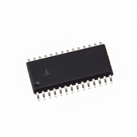
HI5760/6IB Intersil, HI5760/6IB Datasheet

HI5760/6IB
Specifications of HI5760/6IB
Related parts for HI5760/6IB
HI5760/6IB Summary of contents
Page 1
... Ld TSSOP M28.173 125MHz HI5760IAZ - TSSOP (See Note) (Pb-free) HI5760/6IB - SOIC HI5760/6IBZ - SOIC (See Note) (Pb-free) HI5760EVAL1 25 Evaluation Platform * Add “-T” suffix for tape and reel. NOTE: Intersil Pb-free products employ special Pb-free material sets; molding compounds/die attach materials and 100% matte tin plate termination finish, which are RoHS compliant and compatible with both SnPb and Pb-free soldering operations ...
Page 2
Typical Applications Circuit 50Ω FERRITE BEAD + 10µH 10µF 0.1µF Functional Block Diagram (LSB LATCH (MSB) D9 CLK AV ACOM ...
Page 3
Absolute Maximum Ratings Digital Supply Voltage DV to DCOM . . . . . . . . . . . . . . . . . +5.5V DD Analog Supply Voltage AV to ACOM . . . . . . ...
Page 4
... SFDR to Nyquist f CLK f CLK f CLK f CLK f CLK f CLK f CLK f CLK f CLK f CLK AC CHARACTERISTICS - HI5760/6IB, HI5760/6IA - 60MHz Spurious Free Dynamic Range, f CLK SFDR Within a Window f CLK f CLK Total Harmonic Distortion (THD CLK Nyquist f CLK Spurious Free Dynamic Range, f CLK SFDR to Nyquist f CLK ...
Page 5
Electrical Specifications AV DD PARAMETER DIGITAL INPUTS D9-D0, CLK Input Logic High Voltage with (Note 3) 5V Supply Input Logic High Voltage with (Note 3) 3V Supply Input Logic Low Voltage with (Note 3) 5V Supply, ...
Page 6
Typical Performance Curves, 5V Power Supply 0dBFS -12dBFS 50 0 0.2 0.4 0.6 0.8 1 1.2 OUTPUT FREQUENCY (MHz) FIGURE 1. SFDR CLOCK = 5MSPS OUT 80 0dBFS 75 -6dBFS 70 ...
Page 7
Typical Performance Curves, 5V Power Supply 100MSPS -25 -20 -15 -10 AMPLITUDE (dBFS) FIGURE 7. SFDR vs AMPLITUDE ...
Page 8
Typical Performance Curves, 5V Power Supply -20 -20 -30 -30 f Combined Peak Amplitude = 0dBFS -40 -40 AMPLITUDE = 0dBFS 14dB External Analyzer Attenuation -50 -50 -60 ANALYZER ATTENUATION -60 -70 -70 -80 -80 -90 -90 -100 -100 -110 ...
Page 9
Typical Performance Curves, 5V Power Supply FIGURE 19. POWER vs CLOCK RATE, f Typical Performance Curves, 3V Power Supply 0dBFS 65 60 -12dBFS 0.2 0.4 0.6 0.8 1 OUTPUT FREQUENCY (MHz) FIGURE 20. SFDR ...
Page 10
Typical Performance Curves, 3V Power Supply 80 0dBFS -6dBFS 60 -12dBFS OUTPUT FREQUENCY (MHz) FIGURE 24. SFDR CLOCK = 125MSPS OUT ...
Page 11
Typical Performance Curves, 3V Power Supply -40 - TEMPERATURE ( FIGURE 30. SFDR vs TEMPERATURE, CLOCK = 100MSPS -20 -30 -40 -50 -60 ANALYZER ATTENUATION -70 -80 -90 -100 ...
Page 12
Typical Performance Curves, 3V Power Supply 0.4 0.2 0 -0.2 -0.4 0 200 400 600 CODE FIGURE 36. DIFFERENTIAL NONLINEARITY FIGURE 38. POWER vs CLOCK RATE HI5760 (Continued) 0.4 0.2 0 -0.2 -0.4 800 1000 ...
Page 13
Timing Diagrams CLK D9-D0 I OUT t SETT t PD FIGURE 39. OUTPUT SETTLING TIME DIAGRAM CLK t SU D9-D0 I OUT t PD FIGURE 41. PROPAGATION DELAY, SETUP TIME, HOLD TIME AND MINIMUM PULSE WIDTH DIAGRAM 13 HI5760 50% ...
Page 14
Definition of Specifications Integral Linearity Error, INL, is the measure of the worst case point that deviates from a best fit straight line of data values along the transfer curve. Differential Linearity Error, DNL, is the measure of the step ...
Page 15
Digital Inputs and Termination The HI5760 digital inputs are guaranteed to CMOS levels. However, TTL compatibility can be achieved by lowering the supply voltage to 3V due to the digital threshold of the input buffer being approximately half of the ...
Page 16
Pin Descriptions PIN NO. PIN NAME 1-10 D9 (MSB) Through D0 (LSB) 11- SLEEP 16 REFLO 17 REFIO 18 FSADJ 19 COMP1 20 ACOM 21 IOUTB 22 IOUTA DCOM 27 ...
Page 17
Small Outline Plastic Packages (SOIC) N INDEX 0.25(0.010) H AREA E - SEATING PLANE - -C- α 0.10(0.004) 0.25(0.010 NOTES: 1. Symbols are defined in the ...
Page 18
... Accordingly, the reader is cautioned to verify that data sheets are current before placing orders. Information furnished by Intersil is believed to be accurate and reliable. However, no responsibility is assumed by Intersil or its subsidiaries for its use; nor for any infringements of patents or other rights of third parties which may result from its use ...


