EPM240T100C4N Altera, EPM240T100C4N Datasheet - Page 9
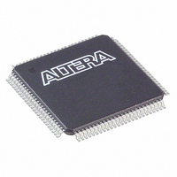
EPM240T100C4N
Manufacturer Part Number
EPM240T100C4N
Description
IC MAX II CPLD 240 LE 100-TQFP
Manufacturer
Altera
Series
MAX® IIr
Specifications of EPM240T100C4N
Programmable Type
In System Programmable
Delay Time Tpd(1) Max
4.7ns
Voltage Supply - Internal
2.5V, 3.3V
Number Of Logic Elements/blocks
240
Number Of Macrocells
192
Number Of I /o
80
Operating Temperature
0°C ~ 85°C
Mounting Type
Surface Mount
Package / Case
100-TQFP, 100-VQFP
Voltage
2.5V, 3.3V
Memory Type
FLASH
Number Of Logic Elements/cells
240
Lead Free Status / RoHS Status
Lead free / RoHS Compliant
Features
-
Other names
544-1963
EPM240T100C4N
EPM240T100C4N
Available stocks
Company
Part Number
Manufacturer
Quantity
Price
Company:

Part Number:
EPM240T100C4N
Manufacturer:
ALTERA
Quantity:
720
Part Number:
EPM240T100C4N
Manufacturer:
ALTERA/阿尔特拉
Quantity:
20 000


Introduction
Functional Description
© October 2008 Altera Corporation
MII51002-2.2
This chapter describes the architecture of the MAX II device and contains the
following sections:
■
■
■
■
■
■
■
■
MAX
implement custom logic. Row and column interconnects provide signal interconnects
between the logic array blocks (LABs).
The logic array consists of LABs, with 10 logic elements (LEs) in each LAB. An LE is a
small unit of logic providing efficient implementation of user logic functions. LABs
are grouped into rows and columns across the device. The MultiTrack interconnect
provides fast granular timing delays between LABs. The fast routing between LEs
provides minimum timing delay for added levels of logic versus globally routed
interconnect structures.
The MAX II device I/O pins are fed by I/O elements (IOE) located at the ends of LAB
rows and columns around the periphery of the device. Each IOE contains a
bidirectional I/O buffer with several advanced features. I/O pins support Schmitt
trigger inputs and various single-ended standards, such as 66-MHz, 32-bit PCI, and
LVTTL.
MAX II devices provide a global clock network. The global clock network consists of
four global clock lines that drive throughout the entire device, providing clocks for all
resources within the device. The global clock lines can also be used for control signals
such as clear, preset, or output enable.
“Functional Description” on page 2–1
“Logic Array Blocks” on page 2–4
“Logic Elements” on page 2–6
“MultiTrack Interconnect” on page 2–12
“Global Signals” on page 2–16
“User Flash Memory Block” on page 2–18
“MultiVolt Core” on page 2–22
“I/O Structure” on page 2–23
®
II devices contain a two-dimensional row- and column-based architecture to
2. MAX II Architecture
MAX II Device Handbook
Related parts for EPM240T100C4N
Image
Part Number
Description
Manufacturer
Datasheet
Request
R

Part Number:
Description:
CYCLONE II STARTER KIT EP2C20N
Manufacturer:
Altera
Datasheet:


Part Number:
Description:
CPLD, EP610 Family, ECMOS Process, 300 Gates, 16 Macro Cells, 16 Reg., 16 User I/Os, 5V Supply, 35 Speed Grade, 24DIP
Manufacturer:
Altera Corporation
Datasheet:
Part Number:
Description:
CPLD, EP610 Family, ECMOS Process, 300 Gates, 16 Macro Cells, 16 Reg., 16 User I/Os, 5V Supply, 15 Speed Grade, 24DIP
Manufacturer:
Altera Corporation
Datasheet:
Part Number:
Description:
Manufacturer:
Altera Corporation
Datasheet:
Part Number:
Description:
CPLD, EP610 Family, ECMOS Process, 300 Gates, 16 Macro Cells, 16 Reg., 16 User I/Os, 5V Supply, 30 Speed Grade, 24DIP
Manufacturer:
Altera Corporation
Datasheet:
Part Number:
Description:
High-performance, low-power erasable programmable logic devices with 8 macrocells, 10ns
Manufacturer:
Altera Corporation
Datasheet:
Part Number:
Description:
High-performance, low-power erasable programmable logic devices with 8 macrocells, 7ns
Manufacturer:
Altera Corporation
Datasheet:
Part Number:
Description:
Classic EPLD
Manufacturer:
Altera Corporation
Datasheet:
Part Number:
Description:
High-performance, low-power erasable programmable logic devices with 8 macrocells, 10ns
Manufacturer:
Altera Corporation
Datasheet:
Part Number:
Description:
Manufacturer:
Altera Corporation
Datasheet:
Part Number:
Description:
Manufacturer:
Altera Corporation
Datasheet:
Part Number:
Description:
Manufacturer:
Altera Corporation
Datasheet:
Part Number:
Description:
CPLD, EP610 Family, ECMOS Process, 300 Gates, 16 Macro Cells, 16 Reg., 16 User I/Os, 5V Supply, 25 Speed Grade, 24DIP
Manufacturer:
Altera Corporation
Datasheet: