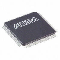
EPM240T100C5 Altera, EPM240T100C5 Datasheet - Page 10

EPM240T100C5
Manufacturer Part Number
EPM240T100C5
Description
IC MAX II CPLD 240 LE 100-TQFP
Manufacturer
Altera
Series
MAX® IIr
Specifications of EPM240T100C5
Programmable Type
In System Programmable
Delay Time Tpd(1) Max
4.7ns
Voltage Supply - Internal
2.5V, 3.3V
Number Of Logic Elements/blocks
240
Number Of Macrocells
192
Number Of I /o
80
Operating Temperature
0°C ~ 85°C
Mounting Type
Surface Mount
Package / Case
100-TQFP, 100-VQFP
Voltage
2.5V, 3.3V
Memory Type
FLASH
Number Of Logic Elements/cells
240
Lead Free Status / RoHS Status
Contains lead / RoHS non-compliant
Features
-
Other names
544-1146
Available stocks
Company
Part Number
Manufacturer
Quantity
Price
Company:
Part Number:
EPM240T100C5
Manufacturer:
ALTERA
Quantity:
9
Company:
Part Number:
EPM240T100C5
Manufacturer:
ALTERA
Quantity:
3 560
Company:
Part Number:
EPM240T100C5
Manufacturer:
ALTERA
Quantity:
4 000
Part Number:
EPM240T100C5M
Manufacturer:
ALTERA/阿尔特拉
Quantity:
20 000
Company:
Part Number:
EPM240T100C5N
Manufacturer:
VISHAY
Quantity:
12 000
Company:
Part Number:
EPM240T100C5N
Manufacturer:
ALTERA
Quantity:
8 903
Part Number:
EPM240T100C5N
Manufacturer:
ALTERA/阿尔特拉
Quantity:
20 000
Part Number:
EPM240T100C5NAH
Manufacturer:
ALTERA/阿尔特拉
Quantity:
20 000
2–2
Figure 2–1. MAX II Device Block Diagram
MAX II Device Handbook
f
MultiTrack
Interconnect
IOE
IOE
IOE
IOE
Figure 2–1
Each MAX II device contains a flash memory block within its floorplan. On the
EPM240 device, this block is located on the left side of the device. On the EPM570,
EPM1270, and EPM2210 devices, the flash memory block is located on the bottom-left
area of the device. The majority of this flash memory storage is partitioned as the
dedicated configuration flash memory (CFM) block. The CFM block provides the non-
volatile storage for all of the SRAM configuration information. The CFM
automatically downloads and configures the logic and I/O at power-up, providing
instant-on operation.
For more information about configuration upon power-up, refer to the
and Power-On Reset in MAX II Devices
A portion of the flash memory within the MAX II device is partitioned into a small
block for user data. This user flash memory (UFM) block provides 8,192 bits of
general-purpose user storage. The UFM provides programmable port connections to
the logic array for reading and writing. There are three LAB rows adjacent to this
block, with column numbers varying by device.
Table 2–1
number of LAB rows and columns adjacent to the flash memory area in the EPM570,
EPM1270, and EPM2210 devices. The long LAB rows are full LAB rows that extend
from one side of row I/O blocks to the other. The short LAB rows are adjacent to the
UFM block; their length is shown as width in LAB columns.
IOE
shows the number of LAB rows and columns in each device, as well as the
shows a functional block diagram of the MAX II device.
Element
Element
Element
Element
Logic
Logic
Logic
Logic
IOE
Interconnect
MultiTrack
IOE
Element
Element
Element
Element
Logic
Logic
Logic
Logic
IOE
chapter in the MAX II Device Handbook.
IOE
Element
Element
Element
Element
Logic
Logic
Logic
Logic
IOE
© October 2008 Altera Corporation
Chapter 2: MAX II Architecture
Logic Array
BLock (LAB)
Functional Description
Hot Socketing


