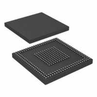
ADSP-BF527KBCZ-6C2 Analog Devices Inc, ADSP-BF527KBCZ-6C2 Datasheet - Page 25

ADSP-BF527KBCZ-6C2
Manufacturer Part Number
ADSP-BF527KBCZ-6C2
Description
IC DSP 16BIT 600MHZ 289CSPBGA
Manufacturer
Analog Devices Inc
Series
Blackfin®r
Type
Fixed Pointr
Datasheets
1.ADSP-BF531SBSTZ400.pdf
(12 pages)
2.ADSP-BF523BBCZ-5A.pdf
(88 pages)
3.ADSP-BF523KBCZ-5C2.pdf
(36 pages)
Specifications of ADSP-BF527KBCZ-6C2
Package / Case
289-CSPBGA
Interface
DMA, Ethernet, I²C, PPI, SPI, SPORT, UART, USB
Clock Rate
600MHz
Non-volatile Memory
ROM (32 kB)
On-chip Ram
132kB
Voltage - I/o
1.8V, 2.5V, 3.3V
Voltage - Core
1.10V
Operating Temperature
0°C ~ 70°C
Mounting Type
Surface Mount
Svhc
No SVHC (18-Jun-2010)
Cache On Chip L1/l2 Memory
48KB
Core Frequency Typ
600MHz
Dsp Type
Core
External Supported Memory
SDRAM, SRAM, FLASH, ROM
Interface Type
SPI, Parallel, 2 Wire
Rohs Compliant
Yes
Mmac
1200
No. Of Pins
289
Package
289CSP-BGA
Maximum Speed
600 MHz
Lead Free Status / RoHS Status
Lead free / RoHS Compliant
For Use With
ADZS-BF527-MPSKIT - BOARD EVAL MEDIA PLAYER BF527ADZS-BF527-EZLITE - BOARD EVAL ADSP-BF527
Lead Free Status / RoHS Status
Lead free / RoHS Compliant, Lead free / RoHS Compliant
Available stocks
Company
Part Number
Manufacturer
Quantity
Price
Company:
Part Number:
ADSP-BF527KBCZ-6C2
Manufacturer:
Analog Devices Inc
Quantity:
10 000
Table 10. Signal Descriptions (Continued)
Signal Name
Port J: Multiplexed Peripherals
Real Time Clock
JTAG Port
Clock
Mode Controls
ADSP-BF523/ADSP-BF525/ADSP-BF527 Voltage
Regulation I/F
ADSP-BF522/ADSP-BF524/ADSP-BF526 Voltage
Regulation I/F
PJ0: PPI_FS1/TMR0
PJ1: PPI_CLK/TMRCLK
PJ2: SCL
PJ3: SDA
RTXI
RTXO
TCK
TDO
TDI
TMS
TRST
EMU
CLKIN
XTAL
CLKBUF
RESET
NMI
BMODE3–0
VR
VR
EXT_WAKE0
SS/PG
EXT_WAKE1
EXT_WAKE0
PG
ADSP-BF522/ADSP-BF523/ADSP-BF524/ADSP-BF525/ADSP-BF526/ADSP-BF527
SEL
OUT
/EXT_WAKE1
Type Function
I/O
I
I/O 5V TWI Serial Clock (This pin is an open-drain output and requires a pull-up
I/O 5V TWI Serial Data (This pin is an open-drain output and requires a pull-up
I
O
I
O
I
I
I
O
I
O
O
I
I
I
I
O
O
A
O
O
A
Rev. B | Page 25 of 88 | May 2010
PPI Frame Sync1/Timer0
PPI Clock/Timer Clock
resistor.
resistor.
RTC Crystal Input (This ball should be pulled low when not used.)
RTC Crystal Output (Does not three-state during hibernate.)
JTAG Clock
JTAG Serial Data Out
JTAG Serial Data In
JTAG Mode Select
JTAG Reset (This ball should be pulled low if the JTAG port is not used.)
Emulation Output
Clock/Crystal Input
Crystal Output (If CLKBUF is enabled, does not three-state during hibernate.)
Buffered XTAL Output (If enabled, does not three-state during hibernate.)
Reset
Nonmaskable Interrupt (This ball should be pulled high when not used.)
Boot Mode Strap 3-0
Internal/External Voltage Regulator Select
External FET Drive/Wake up Indication 1 (Does not three-state during
hibernate.)
Wake up Indication 0 (Does not three-state during hibernate.)
Soft Start/Power Good
Wake up Indication 1 (Does not three-state during hibernate.)
Wake up Indication 0 (Does not three-state during hibernate.)
Power Good (This signal should be pulled low when not used.)
4
4
)
)
Driver
Type
C
E
E
C
C
C
G
C
C
C
1


