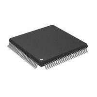
ADSP-2185KSTZ-115 Analog Devices Inc, ADSP-2185KSTZ-115 Datasheet - Page 4

ADSP-2185KSTZ-115
Manufacturer Part Number
ADSP-2185KSTZ-115
Description
IC DSP CONTROLLER 16BIT 100TQFP
Manufacturer
Analog Devices Inc
Series
ADSP-21xxr
Type
Fixed Pointr
Datasheet
1.ADSP-2185BSTZ-133.pdf
(32 pages)
Specifications of ADSP-2185KSTZ-115
Interface
Host Interface, Serial Port
Clock Rate
28.8MHz
Non-volatile Memory
External
On-chip Ram
80kB
Voltage - I/o
5.00V
Voltage - Core
5.00V
Operating Temperature
0°C ~ 70°C
Mounting Type
Surface Mount
Package / Case
100-TQFP, 100-VQFP
Device Core Size
16b
Architecture
Enhanced Harvard
Format
Fixed Point
Clock Freq (max)
28.8MHz
Mips
28.8
Device Input Clock Speed
28.8MHz
Ram Size
80KB
Program Memory Size
Not RequiredKB
Operating Supply Voltage (typ)
5V
Operating Supply Voltage (min)
4.5V
Operating Supply Voltage (max)
5.5V
Operating Temp Range
0C to 70C
Operating Temperature Classification
Commercial
Mounting
Surface Mount
Pin Count
100
Package Type
LQFP
Lead Free Status / RoHS Status
Lead free / RoHS Compliant
ADSP-2185
Common-Mode Pins
Pin
Name(s)
RESET
BR
BG
BGH
DMS
PMS
IOMS
BMS
CMS
RD
WR
IRQ2/
PF7
IRQL0/
PF5
IRQL1/
PF6
IRQE/
PF4
PF3
Mode C/
PF2
Mode B/
PF1
Mode A/
PF0
CLKIN, XTAL 2
CLKOUT
SPORT0
SPORT1/
IRQ1:0
FI, FO
PWD
PWDACK
FL0, FL1, FL2 3
VDD and GND 16
EZ-Port
NOTES
1
2
Interrupt/Flag pins retain both functions concurrently. If IMASK is set to
enable the corresponding interrupts, the DSP will vector to the appropriate
interrupt vector address when the pin is asserted, either by external devices or
set as a programmable flag.
SPORT configuration determined by the DSP System Control Register. Soft-
ware configurable.
#
of
Pins put
1
1
1
1
1
1
1
1
1
1
1
1
1
1
1
1
1
1
1
1
5
5
1
1
9
O
I/O
I/O
O
I/O
Input/
Out-
I
I
O
O
O
O
O
O
O
O
O
I
I/O
I
I/O
I
I/O
I
I/O
I/O
I
I/O
I
I/O
I
I/O
I
I
O
I
Function
Processor Reset Input
Bus Request Input
Bus Grant Output
Bus Grant Hung Output
Data Memory Select Output
Program Memory Select Output
Memory Select Output
Byte Memory Select Output
Combined Memory Select Output
Memory Read Enable Output
Memory Write Enable Output
Edge- or Level-Sensitive
Interrupt Request
Programmable I/O Pin
Level-Sensitive Interrupt Requests
Programmable I/O Pin
Level-Sensitive Interrupt Requests
Programmable I/O Pin
Edge-Sensitive Interrupt Requests
Programmable I/O Pin
Programmable I/O Pin
Mode Select Input—Checked
only During RESET
Programmable I/O Pin During
Normal Operation
Mode Select Input—Checked
only During RESET
Programmable I/O Pin During
Normal Operation
Mode Select Input—Checked
only During RESET
Programmable I/O Pin During
Normal Operation
Clock or Quartz Crystal Input
Processor Clock Output
Serial Port I/O Pins
Serial Port I/O Pins
Edge- or Level-Sensitive Interrupts,
Flag In, Flag Out
Power-Down Control Input
Power-Down Control Output
Output Flags
Power and Ground
For Emulation Use
2
1
1
1
1
–4–
Memory Interface Pins
The ADSP-2185 processor can be used in one of two modes,
Full Memory Mode, which allows BDMA operation with full
external overlay memory and I/O capability, or Host Mode,
which allows IDMA operation with limited external addressing
capabilities. The operating mode is determined by the state of
the Mode C pin during RESET and cannot be changed while
the processor is running.
Full Memory Mode Pins (Mode C = 0)
Pin Name
A13:0
D23:0
Host Mode Pins (Mode C = 1)
Pin Name
IAD15:0
A0
D23:8
IWR
IRD
IAL
IS
IACK
In Host Mode, external peripheral addresses can be decoded using the A0,
CMS, PMS, DMS, and IOMS signals
Setting Memory Mode
Memory Mode selection for the ADSP-2185 is made during
chip reset through the use of the Mode C pin. This pin is multi-
plexed with the DSP’s PF2 pin, so care must be taken in how
the mode selection is made. The two methods for selecting the
value of Mode C are active and passive.
Passive configuration involves the use a pull-up or pull-down
resistor connected to the Mode C pin. To minimize power
consumption, or if the PF2 pin is to be used as an output in the
DSP application, a weak pull-up or pull-down, on the order of
100 k , can be used. This value should be sufficient to pull the
pin to the desired level and still allow the pin to operate as a
programmable flag output without undue strain on the processor’s
output driver. For minimum power consumption during
power-down, reconfigure PF2 to be an input as the pull-up or
pull-down will hold the pin in a known state and will not switch.
Active configuration involves the use of a three-stateable exter-
nal driver connected to the Mode C pin. A driver’s output en-
able should be connected to the DSP’s RESET signal such that
it only drives the PF2 pin when RESET is active (low). After
#
of
Pins
14
24
#
of
Pins
16
1
16
1
1
1
1
1
Input/
Output
O
I/O
Input/
Output
I/O
O
I/O
I
I
I
I
O
Function
Address Output Pins for Pro-
gram, Data, Byte and I/O
Spaces
Data I/O Pins for Program,
Data, Byte and I/O Spaces
(8 MSBs Are Also Used as
Byte Memory Addresses)
Function
IDMA Port Address/Data Bus
Address Pin for External I/O,
Program, Data, or Byte Access
Data I/O Pins for Program,
Data Byte and I/O Spaces
IDMA Write Enable
IDMA Read Enable
IDMA Address Latch Pin
IDMA Select
IDMA Port Acknowledge
REV. 0


