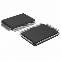
SAA7706H/N107,557 NXP Semiconductors, SAA7706H/N107,557 Datasheet - Page 2

SAA7706H/N107,557
Manufacturer Part Number
SAA7706H/N107,557
Description
IC CAR RADIO DSP 80-QFP
Manufacturer
NXP Semiconductors
Type
Car Signal Processorr
Datasheet
1.SAA7706HN210S518.pdf
(52 pages)
Specifications of SAA7706H/N107,557
Interface
I²C, I²S, LSB, SPDIF
Voltage - I/o
3.30V
Voltage - Core
3.30V
Operating Temperature
-40°C ~ 85°C
Mounting Type
Surface Mount
Package / Case
80-QFP
Lead Free Status / RoHS Status
Lead free / RoHS Compliant
Clock Rate
-
Non-volatile Memory
-
On-chip Ram
-
Other names
935267098557
SAA7706H/N107
SAA7706H/N107
SAA7706H/N107
SAA7706H/N107
Available stocks
Company
Part Number
Manufacturer
Quantity
Price
Company:
Part Number:
SAA7706H/N107,557
Manufacturer:
NXP Semiconductors
Quantity:
10 000
Philips Semiconductors
CONTENTS
1
1.1
1.2
2
3
4
5
6
7
8
8.1
8.1.1
8.1.2
8.1.3
8.1.4
8.1.5
8.1.6
8.2
8.3
8.4
8.4.1
8.4.2
8.4.3
8.5
8.6
8.6.1
8.7
8.7.1
8.7.2
8.7.3
8.7.4
8.7.5
8.7.6
8.8
8.8.1
8.9
8.10
8.11
8.12
8.12.1
8.12.2
2001 Mar 05
Car radio Digital Signal Processor (DSP)
FEATURES
Hardware
Software
APPLICATIONS
GENERAL DESCRIPTION
QUICK REFERENCE DATA
ORDERING INFORMATION
BLOCK DIAGRAM
PINNING
FUNCTIONAL DESCRIPTION
Analog front-end
The realization of common mode input with AIC
Realization of the auxiliary input with volume
control
Realization of the FM input control
Pins VDACN1, VDACN2 and VDACP
Pin VREFAD
Supply of the analog inputs
The signal audio path for input signals CD,
TAPE, AUX, PHONE, NAV and AM
Signal path for level information
Signal path from FM_MPX input to IAC and
stereo decoder
Noise level
Mono or stereo switching
The automatic lock system
DCS clock
The Interference Absorption Circuit (IAC)
General description
The Filter Stream DAC (FSDAC)
Interpolation filter
Noise shaper
Function of pin POM
Power-off plop suppression
Pin VREFDA for internal reference
Supply of the filter stream DAC
Clock circuit and oscillator
Supply of the crystal oscillator
The phase-locked loop circuit to generate the
DSPs and other clocks
Supply of the digital part (V
CL_GEN, audio clock recovery block
External control pins
DSP1
DSP2
DDD3V1
to V
DDD3V4
)
2
8.13
8.14
8.14.1
8.14.2
8.14.3
8.15
8.15.1
8.15.2
8.15.3
8.15.4
8.16
8.17
9
9.1
9.2
9.3
9.4
9.5
9.5.1
9.6
10
11
12
13
14
15
16
17
18
18.1
18.2
18.3
18.4
18.5
19
20
21
22
I
Digital serial inputs/outputs and SPDIF inputs
General description digital serial audio
inputs/outputs
General description SPDIF inputs (SPDIF1 and
SPDIF2)
Digital data stream formats
RDS demodulator (pins RDS_CLOCK
and RDS_DATA)
Clock and data recovery
Timing of clock and data signals
Buffering of RDS data
Buffer interface
DSP reset
Test mode connections (pins TSCAN, RTCB
and SHTCB)
I
Addressing
Slave address (pin A0)
Write cycles
Read cycles
SAA7706H hardware registers
SAA7706H DSPs registers
I
LIMITING VALUES
THERMAL CHARACTERISTICS
CHARACTERISTICS
RDS AND I
I
SOFTWARE DESCRIPTION
APPLICATION DIAGRAM
PACKAGE OUTLINE
SOLDERING
Introduction to soldering surface mount
packages
Reflow soldering
Wave soldering
Manual soldering
Suitability of surface mount IC packages for
wave and reflow soldering methods
DATA SHEET STATUS
DEFINITIONS
DISCLAIMERS
PURCHASE OF PHILIPS I
2
2
2
2
C-bus control (pins SCL and SDA)
C-BUS FORMAT
C-bus memory map specification
C-BUS TIMING
2
S-BUS TIMING
Product specification
SAA7706H
2
C COMPONENTS


