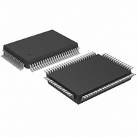
SAA7706H/N107,557 NXP Semiconductors, SAA7706H/N107,557 Datasheet - Page 23

SAA7706H/N107,557
Manufacturer Part Number
SAA7706H/N107,557
Description
IC CAR RADIO DSP 80-QFP
Manufacturer
NXP Semiconductors
Type
Car Signal Processorr
Datasheet
1.SAA7706HN210S518.pdf
(52 pages)
Specifications of SAA7706H/N107,557
Interface
I²C, I²S, LSB, SPDIF
Voltage - I/o
3.30V
Voltage - Core
3.30V
Operating Temperature
-40°C ~ 85°C
Mounting Type
Surface Mount
Package / Case
80-QFP
Lead Free Status / RoHS Status
Lead free / RoHS Compliant
Clock Rate
-
Non-volatile Memory
-
On-chip Ram
-
Other names
935267098557
SAA7706H/N107
SAA7706H/N107
SAA7706H/N107
SAA7706H/N107
Available stocks
Company
Part Number
Manufacturer
Quantity
Price
Company:
Part Number:
SAA7706H/N107,557
Manufacturer:
NXP Semiconductors
Quantity:
10 000
Philips Semiconductors
8.8.1
The power supply connections of the oscillator are
separated from the other supply lines. This is done to
minimize the feedback from the ground bounce of the chip
to the oscillator circuit. Pin V
supply and pin V
resistor plus capacitance is required for proper operating
on pin V
remark in Section 8.10.
8.9
There are several reasons why a PLL circuit is used to
generate the clock for the DSPs:
2001 Mar 05
handbook, full pagewidth
The PLL makes it possible to switch in the rare cases
that tuning on a multiple of the DSP clock frequency
occurs to a slightly higher frequency for the clock of the
DSP. In this way an undisturbed reception with respect
to the DSP clock frequency is possible.
Crystals for the crystal oscillator in the range of twice the
required DSP clock frequency, so approximately
100 MHz, are always third overtone crystals and must
also be manufactured on customer demand. This makes
these crystals expensive. The PLL1 enables the use of
a crystal running in the fundamental mode and also a
general available crystal can be chosen. For this circuit
a 256
type of crystal is widely used.
Car radio Digital Signal Processor (DSP)
The phase-locked loop circuit to generate the
DSPs and other clocks
DD(OSC)
S
44.1 kHz = 11.2896 MHz crystal is chosen. This
UPPLY OF THE CRYSTAL OSCILLATOR
, see Figs 25 and 26. See also important
DD(OSC)
as positive supply. A series
on-chip
off-chip
SS(OSC)
Fig.14 Block diagram of the oscillator in slave mode.
AGC
is used as ground
C3
slave input 3.3 V(p-p)
63
OSC_IN
C1
G m
R bias
23
8.10
The supply voltage on pins V
for at least 10 ms earlier active than the supply voltage
applied to pin V
8.11
When an external I
the FSDAC circuitry needs an 256f
clock is recovered from either the incoming WS of the
digital serial input or the WS derived from the
SPDIF1/SPDIF2 input. There is also a possibility to
provide the chip with an external clock, in that case it must
be a 256f
64
OSC_OUT
0.5V DD(OSC)
Although a multiple of the frequency of the used crystal
of 11.2896 MHz falls within the FM reception band, this
will not disturb the reception because the relatively low
frequency crystal is driven in a controlled way and the
sine wave of the crystal has in the FM reception band
only very minor harmonics.
C2
Supply of the digital part (V
CL_GEN, audio clock recovery block
s
clock with a fixed phase relation to the source.
65
V DD(OSC)
DD(OSC)
clock to circuit
2
S-bus or SPDIF source is connected,
.
62
V SS(OSC)
MGT470
DDD3V1
s
related clock. This
to V
DDD3V1
Product specification
SAA7706H
DDD3V4
to V
must be
DDD3V4
)


