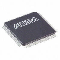
EP1C3T100C7 Altera, EP1C3T100C7 Datasheet - Page 24

EP1C3T100C7
Manufacturer Part Number
EP1C3T100C7
Description
IC CYCLONE FPGA 2910 LE 100-TQFP
Manufacturer
Altera
Series
Cyclone®r
Datasheet
1.EP1C3T144C8.pdf
(106 pages)
Specifications of EP1C3T100C7
Number Of Logic Elements/cells
2910
Number Of Labs/clbs
291
Total Ram Bits
59904
Number Of I /o
65
Voltage - Supply
1.425 V ~ 1.575 V
Mounting Type
Surface Mount
Operating Temperature
0°C ~ 85°C
Package / Case
100-TQFP, 100-VQFP
Lead Free Status / RoHS Status
Contains lead / RoHS non-compliant
Number Of Gates
-
Other names
544-1015
Available stocks
Company
Part Number
Manufacturer
Quantity
Price
Company:
Part Number:
EP1C3T100C7
Manufacturer:
ALTERA
Quantity:
455
Part Number:
EP1C3T100C7
Manufacturer:
ALTERA
Quantity:
20 000
Company:
Part Number:
EP1C3T100C7N
Manufacturer:
ALTERA
Quantity:
364
Part Number:
EP1C3T100C7N
Manufacturer:
ALTERA
Quantity:
20 000
Cyclone Device Handbook, Volume 1
Embedded
Memory
2–18
Preliminary
The Cyclone embedded memory consists of columns of M4K memory
blocks. EP1C3 and EP1C6 devices have one column of M4K blocks, while
EP1C12 and EP1C20 devices have two columns (refer to
page 1–1
various types of memory with or without parity, including true dual-port,
simple dual-port, and single-port RAM, ROM, and FIFO buffers. The
M4K blocks support the following features:
■
■
■
■
■
■
■
■
■
■
■
1
Memory Modes
The M4K memory blocks include input registers that synchronize writes
and output registers to pipeline designs and improve system
performance. M4K blocks offer a true dual-port mode to support any
combination of two-port operations: two reads, two writes, or one read
and one write at two different clock frequencies.
dual-port memory.
Figure 2–12. True Dual-Port Memory Configuration
4,608 RAM bits
250 MHz performance
True dual-port memory
Simple dual-port memory
Single-port memory
Byte enable
Parity bits
Shift register
FIFO buffer
ROM
Mixed clock mode
Violating the setup or hold time on the address registers could
corrupt the memory contents. This applies to both read and
write operations.
for total RAM bits per density). Each M4K block can implement
data
address
wren
clocken
q
aclr
A
clock
[ ]
A
A
A
[ ]
A
A
A
[ ]
A
B
address
clocken
clock
data
wren
Figure 2–12
aclr
q
B
B
B
B
[ ]
[ ]
[ ]
B
B
B
Altera Corporation
Table 1–1 on
shows true
May 2008


