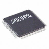
EP1C3T100C7 Altera, EP1C3T100C7 Datasheet - Page 82

EP1C3T100C7
Manufacturer Part Number
EP1C3T100C7
Description
IC CYCLONE FPGA 2910 LE 100-TQFP
Manufacturer
Altera
Series
Cyclone®r
Datasheet
1.EP1C3T144C8.pdf
(106 pages)
Specifications of EP1C3T100C7
Number Of Logic Elements/cells
2910
Number Of Labs/clbs
291
Total Ram Bits
59904
Number Of I /o
65
Voltage - Supply
1.425 V ~ 1.575 V
Mounting Type
Surface Mount
Operating Temperature
0°C ~ 85°C
Package / Case
100-TQFP, 100-VQFP
Lead Free Status / RoHS Status
Contains lead / RoHS non-compliant
Number Of Gates
-
Other names
544-1015
Available stocks
Company
Part Number
Manufacturer
Quantity
Price
Company:
Part Number:
EP1C3T100C7
Manufacturer:
ALTERA
Quantity:
455
Part Number:
EP1C3T100C7
Manufacturer:
ALTERA
Quantity:
20 000
Company:
Part Number:
EP1C3T100C7N
Manufacturer:
ALTERA
Quantity:
364
Part Number:
EP1C3T100C7N
Manufacturer:
ALTERA
Quantity:
20 000
Cyclone Device Handbook, Volume 1
4–12
Preliminary
t
t
t
t
t
t
t
t
t
t
t
t
t
t
t
t
t
t
t
t
t
t
t
t
t
t
t
t
SU
H
CO
PIN2COMBOUT_R
PIN2COMBOUT_C
COMBIN2PIN_R
COMBIN2PIN_C
CLR
PRE
CLKHL
M4KRC
M4KWC
M4KWERESU
M4KWEREH
M4KBESU
M4KBEH
M4KDATAASU
M4KDATAAH
M4KADDRASU
M4KADDRAH
M4KDATABSU
M4KDATABH
M4KADDRBSU
M4KADDRBH
M4KDATACO1
M4KDATACO2
M4KCLKHL
M4KCLR
Table 4–22. IOE Internal Timing Microparameter Descriptions
Table 4–23. M4K Block Internal Timing Microparameter Descriptions
Symbol
Symbol
Synchronous read cycle time
Synchronous write cycle time
Write or read enable setup time before clock
Write or read enable hold time after clock
Byte enable setup time before clock
Byte enable hold time after clock
A port data setup time before clock
A port data hold time after clock
A port address setup time before clock
A port address hold time after clock
B port data setup time before clock
B port data hold time after clock
B port address setup time before clock
B port address hold time after clock
Clock-to-output delay when using output registers
Clock-to-output delay without output registers
Minimum clock high or low time
Minimum clear pulse width
IOE input and output register setup time before clock
IOE input and output register hold time after clock
IOE input and output register clock-to-output delay
Row input pin to IOE combinatorial output
Column input pin to IOE combinatorial output
Row IOE data input to combinatorial output pin
Column IOE data input to combinatorial output pin
Minimum clear pulse width
Minimum preset pulse width
Minimum clock high or low time
Parameter
Parameter
Altera Corporation
May 2008


