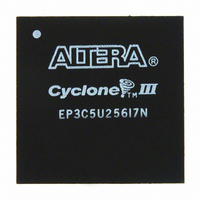
EP3C5U256I7N Altera, EP3C5U256I7N Datasheet - Page 50

EP3C5U256I7N
Manufacturer Part Number
EP3C5U256I7N
Description
IC CYCLONE III FPGA 5K 256 UBGA
Manufacturer
Altera
Series
Cyclone® IIIr
Datasheets
1.EP3C5F256C8N.pdf
(5 pages)
2.EP3C5F256C8N.pdf
(34 pages)
3.EP3C5F256C8N.pdf
(66 pages)
4.EP3C5F256C8N.pdf
(14 pages)
5.EP3C5F256C8N.pdf
(76 pages)
6.EP3C5U256I7N.pdf
(274 pages)
Specifications of EP3C5U256I7N
Number Of Logic Elements/cells
5136
Number Of Labs/clbs
321
Total Ram Bits
423936
Number Of I /o
182
Voltage - Supply
1.15 V ~ 1.25 V
Mounting Type
Surface Mount
Operating Temperature
-40°C ~ 100°C
Package / Case
256-UBGA
Family Name
Cyclone III
Number Of Logic Blocks/elements
5136
# I/os (max)
182
Frequency (max)
437.5MHz
Process Technology
65nm
Operating Supply Voltage (typ)
1.2V
Logic Cells
5136
Ram Bits
423936
Operating Supply Voltage (min)
1.15V
Operating Supply Voltage (max)
1.25V
Operating Temp Range
-40C to 100C
Operating Temperature Classification
Industrial
Mounting
Surface Mount
Pin Count
256
Package Type
UFBGA
For Use With
544-2601 - KIT DEV CYCLONE III LS EP3CLS200544-2411 - KIT DEV NIOS II CYCLONE III ED.
Lead Free Status / RoHS Status
Lead free / RoHS Compliant
Number Of Gates
-
Lead Free Status / Rohs Status
Compliant
Other names
544-2560
Available stocks
Company
Part Number
Manufacturer
Quantity
Price
Company:
Part Number:
EP3C5U256I7N
Manufacturer:
ALTERA21
Quantity:
201
Part Number:
EP3C5U256I7N
Manufacturer:
ALTERA/阿尔特拉
Quantity:
20 000
- EP3C5F256C8N PDF datasheet
- EP3C5F256C8N PDF datasheet #2
- EP3C5F256C8N PDF datasheet #3
- EP3C5F256C8N PDF datasheet #4
- EP3C5F256C8N PDF datasheet #5
- EP3C5U256I7N PDF datasheet #6
- Current page: 50 of 274
- Download datasheet (6Mb)
3–14
Figure 3–13. Cyclone III Device Family Shift Register Mode Configuration
ROM Mode
FIFO Buffer Mode
Cyclone III Device Handbook, Volume 1
f
w × m × n Shift Register
W
W
W
W
Figure 3–13
register mode.
Cyclone III device family M9K memory blocks support ROM mode. A .mif initializes
the ROM contents of these blocks. The address lines of the ROM are registered. The
outputs can be registered or unregistered. The ROM read operation is identical to the
read operation in the single-port RAM configuration.
Cyclone III device family M9K memory blocks support single-clock or dual-clock
FIFO buffers. Dual clock FIFO buffers are useful when transferring data from one
clock domain to another clock domain. Cyclone III device family M9K memory blocks
do not support simultaneous read and write from an empty FIFO buffer.
For more information about FIFO buffers, refer to the
Megafunction User
m-Bit Shift Register
m-Bit Shift Register
m-Bit Shift Register
m-Bit Shift Register
shows the Cyclone III device family M9K memory block in the shift
Guide.
Chapter 3: Memory Blocks in the Cyclone III Device Family
W
W
W
W
Single- and Dual-Clock FIFO
© December 2009 Altera Corporation
n Number of Taps
Memory Modes
Related parts for EP3C5U256I7N
Image
Part Number
Description
Manufacturer
Datasheet
Request
R

Part Number:
Description:
Cyclone III Device Data Sheet
Manufacturer:
ALTERA [Altera Corporation]
Datasheet:

Part Number:
Description:
CYCLONE II STARTER KIT EP2C20N
Manufacturer:
Altera
Datasheet:

Part Number:
Description:
CPLD, EP610 Family, ECMOS Process, 300 Gates, 16 Macro Cells, 16 Reg., 16 User I/Os, 5V Supply, 35 Speed Grade, 24DIP
Manufacturer:
Altera Corporation
Datasheet:

Part Number:
Description:
CPLD, EP610 Family, ECMOS Process, 300 Gates, 16 Macro Cells, 16 Reg., 16 User I/Os, 5V Supply, 15 Speed Grade, 24DIP
Manufacturer:
Altera Corporation
Datasheet:

Part Number:
Description:
Manufacturer:
Altera Corporation
Datasheet:

Part Number:
Description:
CPLD, EP610 Family, ECMOS Process, 300 Gates, 16 Macro Cells, 16 Reg., 16 User I/Os, 5V Supply, 30 Speed Grade, 24DIP
Manufacturer:
Altera Corporation
Datasheet:

Part Number:
Description:
High-performance, low-power erasable programmable logic devices with 8 macrocells, 10ns
Manufacturer:
Altera Corporation
Datasheet:

Part Number:
Description:
High-performance, low-power erasable programmable logic devices with 8 macrocells, 7ns
Manufacturer:
Altera Corporation
Datasheet:

Part Number:
Description:
Classic EPLD
Manufacturer:
Altera Corporation
Datasheet:

Part Number:
Description:
High-performance, low-power erasable programmable logic devices with 8 macrocells, 10ns
Manufacturer:
Altera Corporation
Datasheet:

Part Number:
Description:
Manufacturer:
Altera Corporation
Datasheet:

Part Number:
Description:
Manufacturer:
Altera Corporation
Datasheet:

Part Number:
Description:
Manufacturer:
Altera Corporation
Datasheet:


