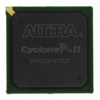
EP2C35F672C6 Altera, EP2C35F672C6 Datasheet - Page 72

EP2C35F672C6
Manufacturer Part Number
EP2C35F672C6
Description
IC CYCLONE II FPGA 33K 672-FBGA
Manufacturer
Altera
Series
Cyclone® IIr
Datasheet
1.EP2C5T144C8N.pdf
(168 pages)
Specifications of EP2C35F672C6
Number Of Logic Elements/cells
33216
Number Of Labs/clbs
2076
Total Ram Bits
483840
Number Of I /o
475
Voltage - Supply
1.15 V ~ 1.25 V
Mounting Type
Surface Mount
Operating Temperature
0°C ~ 85°C
Package / Case
672-FBGA
Family Name
Cyclone® II
Number Of Logic Blocks/elements
33216
# I/os (max)
475
Frequency (max)
500MHz
Process Technology
90nm
Operating Supply Voltage (typ)
1.2V
Logic Cells
33216
Ram Bits
483840
Operating Supply Voltage (min)
1.15V
Operating Supply Voltage (max)
1.25V
Operating Temp Range
0C to 85C
Operating Temperature Classification
Commercial
Mounting
Surface Mount
Pin Count
672
Package Type
FBGA
For Use With
P0301 - DE2 CALL FOR ACADEMIC PRICING544-1733 - PCI KIT W/CYCLONE II EP2C35N649-1001 - KIT DEV CYCLONE II PCI EXPRESS
Lead Free Status / RoHS Status
Contains lead / RoHS non-compliant
Number Of Gates
-
Lead Free Status / Rohs Status
Not Compliant
Other names
544-1087
EP2C35F672C6ES
EP2C35F672C6ES
Available stocks
Company
Part Number
Manufacturer
Quantity
Price
Company:
Part Number:
EP2C35F672C6N
Manufacturer:
ALTERA
Quantity:
170
I/O Structure & Features
2–60
Cyclone II Device Handbook, Volume 1
Table 2–20. Cyclone II MultiVolt I/O Support (Part 1 of 2)
V
CCIO
1.5
1.8
2.5
(V)
v
1.5 V
v
(4)
1.8 V
v
v
standards (e.g., SSTL-2) independently. If an I/O bank does not use
voltage-referenced standards, the VREF pins are available as user I/O
pins.
Each I/O bank can support multiple standards with the same V
input and output pins. For example, when V
support LVTTL, LVCMOS, and 3.3-V PCI for inputs and outputs.
Voltage-referenced standards can be supported in an I/O bank using any
number of single-ended or differential standards as long as they use the
same V
MultiVolt I/O Interface
The Cyclone II architecture supports the MultiVolt I/O interface feature,
which allows Cyclone II devices in all packages to interface with systems
of different supply voltages. Cyclone II devices have one set of V
(VCCINT) that power the internal device logic array and input buffers that
use the LVPECL, LVDS, HSTL, or SSTL I/O standards. Cyclone II devices
also have four or eight sets of VCC pins (VCCIO) that power the I/O
output drivers and input buffers that use the LVTTL, LVCMOS, or PCI
I/O standards.
The Cyclone II VCCINT pins must always be connected to a 1.2-V power
supply. If the V
and 3.3-V tolerant. The VCCIO pins can be connected to either a 1.5-V,
1.8-V, 2.5-V, or 3.3-V power supply, depending on the output
requirements. The output levels are compatible with systems of the same
voltage as the power supply (i.e., when VCCIO pins are connected to a
1.5-V power supply, the output levels are compatible with 1.5-V systems).
When VCCIO pins are connected to a 3.3-V power supply, the output high
is 3.3-V and is compatible with 3.3-V systems.
Cyclone II MultiVolt I/O support.
Input Signal
REF
v
v
2.5 V
v
and a compatible V
(2)
(2)
CCINT
v
v
3.3 V
level is 1.2 V, then input pins are 1.5-V, 1.8-V, 2.5-V,
v
(2)
(2)
CCIO
v
v
Note (1)
1.5 V
v
(3)
(5)
value.
v
1.8 V
v
Output Signal
CCIO
(5)
Table 2–20
is 3.3-V, a bank can
2.5 V
Altera Corporation
v
summarizes
February 2007
CCIO
CC
3.3 V
pins
for


