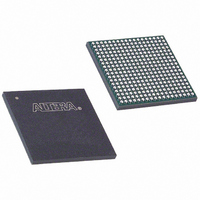
EP1C20F324I7 Altera, EP1C20F324I7 Datasheet - Page 60

EP1C20F324I7
Manufacturer Part Number
EP1C20F324I7
Description
IC CYCLONE FPGA 20K LE 324-FBGA
Manufacturer
Altera
Series
Cyclone®r
Datasheet
1.EP1C3T144C8.pdf
(106 pages)
Specifications of EP1C20F324I7
Number Of Logic Elements/cells
20060
Number Of Labs/clbs
2006
Total Ram Bits
294912
Number Of I /o
233
Voltage - Supply
1.425 V ~ 1.575 V
Mounting Type
Surface Mount
Operating Temperature
-40°C ~ 100°C
Package / Case
324-FBGA
Family Name
Cyclone®
Number Of Logic Blocks/elements
20060
# I/os (max)
233
Frequency (max)
320.1MHz
Process Technology
0.13um (CMOS)
Operating Supply Voltage (typ)
1.5V
Logic Cells
20060
Ram Bits
294912
Operating Supply Voltage (min)
1.425V
Operating Supply Voltage (max)
1.575V
Operating Temp Range
-40C to 100C
Operating Temperature Classification
Industrial
Mounting
Surface Mount
Pin Count
324
Package Type
FBGA
Lead Free Status / RoHS Status
Contains lead / RoHS non-compliant
Number Of Gates
-
Lead Free Status / Rohs Status
Not Compliant
Other names
544-1041
Available stocks
Company
Part Number
Manufacturer
Quantity
Price
Part Number:
EP1C20F324I7
Manufacturer:
ALTERA/阿尔特拉
Quantity:
20 000
Company:
Part Number:
EP1C20F324I7N
Manufacturer:
ALTERA/31
Quantity:
318
Cyclone Device Handbook, Volume 1
2–54
Preliminary
Each I/O bank can support multiple standards with the same V
input and output pins. For example, when V
support LVTTL, LVCMOS, 3.3-V PCI, and SSTL-3 for inputs and outputs.
LVDS I/O Pins
A subset of pins in all four I/O banks supports LVDS interfacing. These
dual-purpose LVDS pins require an external-resistor network at the
transmitter channels in addition to 100-Ω termination resistors on
receiver channels. These pins do not contain dedicated serialization or
deserialization circuitry; therefore, internal logic performs serialization
and deserialization functions.
Table 2–13
device density.
MultiVolt I/O Interface
The Cyclone architecture supports the MultiVolt I/O interface feature,
which allows Cyclone devices in all packages to interface with systems of
different supply voltages. The devices have one set of V
internal operation and input buffers (V
output drivers (V
Note to
(1)
EP1C3
EP1C4
EP1C6
EP1C12
EP1C20
Table 2–13. Cyclone Device LVDS Channels
EP1C3 devices in the 100-pin TQFP package do not support the LVDS I/O
standard.
Device
Table
shows the total number of supported LVDS channels per
2–13:
CCIO
).
Pin Count
100
144
324
400
144
240
256
240
256
324
324
400
CCINT
), and four sets for I/O
Number of LVDS Channels
CCIO
is 3.3-V, a bank can
Altera Corporation
103
129
103
129
(1)
34
29
72
72
66
72
95
CC
pins for
May 2008
CCIO
for


