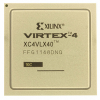
XC4VLX40-10FFG1148C Xilinx Inc, XC4VLX40-10FFG1148C Datasheet - Page 47

XC4VLX40-10FFG1148C
Manufacturer Part Number
XC4VLX40-10FFG1148C
Description
IC FPGA VIRTEX-4 40K 1148-FBGA
Manufacturer
Xilinx Inc
Series
Virtex™-4r
Specifications of XC4VLX40-10FFG1148C
Total Ram Bits
1769472
Number Of Logic Elements/cells
41472
Number Of Labs/clbs
4608
Number Of I /o
640
Voltage - Supply
1.14 V ~ 1.26 V
Mounting Type
Surface Mount
Operating Temperature
0°C ~ 85°C
Package / Case
1148-BBGA, FCBGA
No. Of Logic Blocks
4608
No. Of Macrocells
41472
Family Type
Virtex-4
No. Of Speed Grades
10
No. Of I/o's
640
Clock Management
DCM
Core Supply
RoHS Compliant
Lead Free Status / RoHS Status
Lead free / RoHS Compliant
Number Of Gates
-
Lead Free Status / RoHS Status
Lead free / RoHS Compliant
Other names
122-1491
Available stocks
Company
Part Number
Manufacturer
Quantity
Price
Company:
Part Number:
XC4VLX40-10FFG1148C
Manufacturer:
XILINX
Quantity:
1 238
Company:
Part Number:
XC4VLX40-10FFG1148C
Manufacturer:
Xilinx Inc
Quantity:
10 000
Part Number:
XC4VLX40-10FFG1148C
Manufacturer:
XILINX/赛灵思
Quantity:
20 000
Table 57: Global Clock Setup and Hold for LVCMOS25 Standard, with DCM in Source-Synchronous Mode
DS302 (v3.7) September 9, 2009
Product Specification
Notes:
1.
2.
Example Data Input Setup and Hold Times Relative to a Forwarded Clock Input Pin,
situations where clock and data inputs conform to different standards, adjust the setup and hold values accordingly using the values
shown in
T
The timing values were measured using the fine-phase adjustment feature of the DCM. These measurements include CLK0 DCM jitter. Package
skew is not included in these measurements.
IFF = Input Flip-Flop
T
Symbol
PSDCM_0
PHDCM_0
IOB Switching Characteristics
/
No Delay Global Clock and IFF
Source-Synchronous Mode
Description
(1,2)
, page
19.
(2)
with DCM in
www.xilinx.com
Virtex-4 FPGA Data Sheet: DC and Switching Characteristics
XC4VFX100
XC4VFX140
XC4VLX100
XC4VLX160
XC4VLX200
XC4VSX25
XC4VSX35
XC4VSX55
XC4VFX12
XC4VFX20
XC4VFX40
XC4VFX60
XC4VLX15
XC4VLX25
XC4VLX40
XC4VLX60
XC4VLX80
Device
(1)
Using DCM and Global Clock Buffer. For
–0.33
–0.29
–0.37
–0.32
–0.38
–0.31
–0.31
–0.32
–0.37
–0.32
–0.26
–0.31
–0.35
–0.43
–0.38
0.73
0.86
0.90
1.02
1.18
1.24
1.50
0.95
1.04
1.22
0.73
0.92
1.26
1.39
1.55
–
N/A
N/A
12
Speed Grade
–0.33
–0.29
–0.37
–0.32
–0.38
–0.31
–0.31
–0.31
–0.32
–0.37
–0.32
–0.26
–0.31
–0.35
–0.43
–0.38
–0.44
0.88
0.97
1.04
1.15
1.34
1.41
1.69
1.97
1.07
1.17
1.36
0.86
1.03
1.41
1.56
1.75
2.03
–
11
–0.33
–0.29
–0.37
–0.32
–0.38
–0.31
–0.31
–0.31
–0.32
–0.37
–0.32
–0.26
–0.31
–0.35
–0.43
–0.38
–0.44
1.03
1.09
1.19
1.29
1.50
1.57
1.89
2.19
1.17
1.31
1.52
0.96
1.14
1.74
1.96
2.25
–
156
10
Units
ns
ns
ns
ns
ns
ns
ns
ns
ns
ns
ns
ns
ns
ns
ns
ns
ns
47


