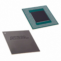
EPF10K100ABC356-3 Altera, EPF10K100ABC356-3 Datasheet - Page 41

EPF10K100ABC356-3
Manufacturer Part Number
EPF10K100ABC356-3
Description
IC FLEX 10KA FPGA 100K 356-BGA
Manufacturer
Altera
Series
FLEX-10K®r
Datasheet
1.EPF10K10ATC100-3.pdf
(128 pages)
Specifications of EPF10K100ABC356-3
Number Of Logic Elements/cells
624
Number Of Labs/clbs
624
Total Ram Bits
24576
Number Of I /o
274
Number Of Gates
158000
Voltage - Supply
3 V ~ 3.6 V
Mounting Type
Surface Mount
Operating Temperature
0°C ~ 85°C
Package / Case
356-BGA
Family Name
FLEX 10KA
Number Of Usable Gates
100000
Number Of Logic Blocks/elements
4992
# Registers
1218
# I/os (max)
274
Frequency (max)
125MHz
Process Technology
CMOS
Operating Supply Voltage (typ)
3.3V
Logic Cells
4992
Ram Bits
24567
Device System Gates
158000
Operating Supply Voltage (min)
3V
Operating Supply Voltage (max)
3.6V
Operating Temp Range
0C to 70C
Operating Temperature Classification
Commercial
Mounting
Surface Mount
Pin Count
356
Package Type
BGA
Lead Free Status / RoHS Status
Contains lead / RoHS non-compliant
Other names
544-2191
Available stocks
Company
Part Number
Manufacturer
Quantity
Price
Company:
Part Number:
EPF10K100ABC356-3
Manufacturer:
ALTERA
Quantity:
36
Company:
Part Number:
EPF10K100ABC356-3
Manufacturer:
MAXIM
Quantity:
304
Company:
Part Number:
EPF10K100ABC356-3N
Manufacturer:
ALTERA
Quantity:
1 259
Altera Corporation
SAMPLE/PRELOAD
EXTEST
BYPASS
USERCODE
IDCODE
ICR Instructions
Table 13. FLEX 10K JTAG Instructions
JTAG Instruction
Allows a snapshot of signals at the device pins to be captured and examined during
normal device operation, and permits an initial data pattern output at the device pins.
Allows the external circuitry and board-level interconnections to be tested by forcing a
test pattern at the output pins and capturing test results at the input pins.
Places the 1-bit bypass register between the TDI and TDO pins, which allows the BST
data to pass synchronously through a selected device to adjacent devices during normal
device operation.
Selects the user electronic signature (USERCODE) register and places it between the
TDI and TDO pins, allowing the USERCODE to be serially shifted out of TDO.
Selects the IDCODE register and places it between TDI and TDO, allowing the IDCODE
to be serially shifted out of TDO.
These instructions are used when configuring a FLEX 10K device via JTAG ports with a
BitBlaster, or ByteBlasterMV or MasterBlaster download cable, or using a Jam File
(.jam) or Jam Byte-Code File (.jbc) via an embedded processor.
The instruction register length of FLEX 10K devices is 10 bits. The
USERCODE register length in FLEX 10K devices is 32 bits; 7 bits are
determined by the user, and 25 bits are predetermined.
show the boundary-scan register length and device IDCODE information
for FLEX 10K devices.
Table 14. FLEX 10K Boundary-Scan Register Length
FLEX 10K Embedded Programmable Logic Device Family Data Sheet
EPF10K10, EPF10K10A
EPF10K20
EPF10K30, EPF10K30A
EPF10K40
EPF10K50, EPF10K50V
EPF10K70
EPF10K100, EPF10K100A
EPF10K130V
EPF10K250A
Device
Description
Register Length
Boundary-Scan
Tables 14
1,104
1,248
1,440
1,440
480
624
768
864
960
and
41
15


