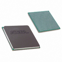
EP2S30F672C5 Altera, EP2S30F672C5 Datasheet - Page 227

EP2S30F672C5
Manufacturer Part Number
EP2S30F672C5
Description
IC STRATIX II FPGA 30K 672-FBGA
Manufacturer
Altera
Series
Stratix® IIr
Datasheet
1.EP2S15F484I4N.pdf
(238 pages)
Specifications of EP2S30F672C5
Number Of Logic Elements/cells
33880
Number Of Labs/clbs
1694
Total Ram Bits
1369728
Number Of I /o
500
Voltage - Supply
1.15 V ~ 1.25 V
Mounting Type
Surface Mount
Operating Temperature
0°C ~ 85°C
Package / Case
672-FBGA
Family Name
Stratix II
Number Of Logic Blocks/elements
33880
# I/os (max)
500
Frequency (max)
609.76MHz
Process Technology
90nm (CMOS)
Operating Supply Voltage (typ)
1.2V
Logic Cells
33880
Ram Bits
1369728
Operating Supply Voltage (min)
1.15V
Operating Supply Voltage (max)
1.25V
Operating Temp Range
0C to 85C
Operating Temperature Classification
Commercial
Mounting
Surface Mount
Pin Count
672
Package Type
FBGA
Lead Free Status / RoHS Status
Contains lead / RoHS non-compliant
Number Of Gates
-
Lead Free Status / Rohs Status
Not Compliant
Other names
544-1126
Available stocks
Company
Part Number
Manufacturer
Quantity
Price
Company:
Part Number:
EP2S30F672C5K
Manufacturer:
ALTERA
Quantity:
220
Company:
Part Number:
EP2S30F672C5N
Manufacturer:
ALTERA
Quantity:
238
Part Number:
EP2S30F672C5N
Manufacturer:
ALTERA/阿尔特拉
Quantity:
20 000
PLL Timing
Specifications
Altera Corporation
April 2011
f
f
f
f
t
t
t
f
t
f
t
f
I N
I N P F D
I N D U T Y
E I N D U T Y
I N J I T T E R
O U T J I T T E R
F C O M P
O U T
O U T D U T Y
S C A N C L K
C O N F I G P L L
O U T _ E X T
Table 5–92. Enhanced PLL Specifications (Part 1 of 2)
Name
Input clock frequency
Input frequency to the
PFD
Input clock duty cycle
External feedback
input clock duty cycle
Input or external
feedback clock input
jitter tolerance in
terms of period jitter.
Bandwidth ≤
0.85 MHz
Input or external
feedback clock input
jitter tolerance in
terms of period jitter.
Bandwidth >
0.85 MHz
Dedicated clock
output period jitter
External feedback
compensation time
Output frequency for
internal global or
regional clock
Duty cycle for external
clock output (when set
to 50%).
Scanclk frequency
Time required to
reconfigure scan
chains for enhanced
PLLs
PLL external clock
output frequency
Description
Tables 5–92
operating in both the commercial junction temperature range (0 to 85 °C)
and the industrial junction temperature range (–40 to 100 °C).
and
Min
1.5
1.5
(2)
(2)
40
40
45
2
2
5–93
174/f
describe the Stratix II PLL specifications when
S C A N C L K
Typ
0.5
1.0
50
250 ps for ≥ 100 MHz
25 mUI for < 100 MHz
Stratix II Device Handbook, Volume 1
DC & Switching Characteristics
550.0
550.0
Max
500
420
100
60
60
10
55
(1)
outclk
outclk
ps or mUI
ns (p-p)
ns (p-p)
(p-p)
MHz
MHz
MHz
MHz
MHz
Unit
ns
ns
%
%
%
5–91


