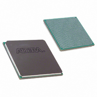
EP2S30F672C5 Altera, EP2S30F672C5 Datasheet - Page 99

EP2S30F672C5
Manufacturer Part Number
EP2S30F672C5
Description
IC STRATIX II FPGA 30K 672-FBGA
Manufacturer
Altera
Series
Stratix® IIr
Datasheet
1.EP2S15F484I4N.pdf
(238 pages)
Specifications of EP2S30F672C5
Number Of Logic Elements/cells
33880
Number Of Labs/clbs
1694
Total Ram Bits
1369728
Number Of I /o
500
Voltage - Supply
1.15 V ~ 1.25 V
Mounting Type
Surface Mount
Operating Temperature
0°C ~ 85°C
Package / Case
672-FBGA
Family Name
Stratix II
Number Of Logic Blocks/elements
33880
# I/os (max)
500
Frequency (max)
609.76MHz
Process Technology
90nm (CMOS)
Operating Supply Voltage (typ)
1.2V
Logic Cells
33880
Ram Bits
1369728
Operating Supply Voltage (min)
1.15V
Operating Supply Voltage (max)
1.25V
Operating Temp Range
0C to 85C
Operating Temperature Classification
Commercial
Mounting
Surface Mount
Pin Count
672
Package Type
FBGA
Lead Free Status / RoHS Status
Contains lead / RoHS non-compliant
Number Of Gates
-
Lead Free Status / Rohs Status
Not Compliant
Other names
544-1126
Available stocks
Company
Part Number
Manufacturer
Quantity
Price
Company:
Part Number:
EP2S30F672C5K
Manufacturer:
ALTERA
Quantity:
220
Company:
Part Number:
EP2S30F672C5N
Manufacturer:
ALTERA
Quantity:
238
Part Number:
EP2S30F672C5N
Manufacturer:
ALTERA/阿尔特拉
Quantity:
20 000
Altera Corporation
May 2007
Note to
(1)
Series termination with
calibration
Parallel termination with
calibration
Differential termination
Table 2–17. On-Chip Termination Support by I/O Banks (Part 2 of 2)
On-Chip Termination Support
Clock pins CLK1, CLK3, CLK9, CLK11, and pins FPLL[7..10]CLK do not support differential on-chip
termination. Clock pins CLK0, CLK2, CLK8, and CLK10 do support differential on-chip termination. Clock pins in
the top and bottom banks (CLK[4..7, 12..15]) do not support differential on-chip termination.
Table
2–17:
(1)
3.3-V LVTTL
3.3-V LVCMOS
2.5-V LVTTL
2.5-V LVCMOS
1.8-V LVTTL
1.8-V LVCMOS
1.5-V LVTTL
1.5-V LVCMOS
SSTL-2 Class I and II
SSTL-18 Class I and II
1.8-V HSTL Class I
1.8-V HSTL Class II
1.5-V HSTL Class I
1.2-V HSTL
SSTL-2 Class I and II
SSTL-18 Class I and II
1.8-V HSTL Class I
1.8-V HSTL Class II
1.5-V HSTL Class I and II
1.2-V HSTL
LVDS
HyperTransport technology
I/O Standard Support
Top & Bottom Banks
Stratix II Device Handbook, Volume 1
v
v
v
v
v
v
v
v
v
v
v
v
v
v
v
v
v
v
v
v
Stratix II Architecture
Left & Right Banks
v
v
2–91


