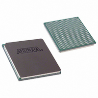
EP3C120F780I7 Altera, EP3C120F780I7 Datasheet - Page 140

EP3C120F780I7
Manufacturer Part Number
EP3C120F780I7
Description
IC CYCLONE III FPGA 120K 780FBGA
Manufacturer
Altera
Series
Cyclone® IIIr
Datasheets
1.EP3C5F256C8N.pdf
(5 pages)
2.EP3C5F256C8N.pdf
(34 pages)
3.EP3C5F256C8N.pdf
(66 pages)
4.EP3C5F256C8N.pdf
(14 pages)
5.EP3C5F256C8N.pdf
(76 pages)
6.EP3C120F780I7.pdf
(274 pages)
Specifications of EP3C120F780I7
Number Of Logic Elements/cells
119088
Number Of Labs/clbs
7443
Total Ram Bits
3981312
Number Of I /o
531
Voltage - Supply
1.15 V ~ 1.25 V
Mounting Type
Surface Mount
Operating Temperature
-40°C ~ 100°C
Package / Case
780-FBGA
Family Name
Cyclone III
Number Of Logic Blocks/elements
119088
# I/os (max)
531
Frequency (max)
437.5MHz
Process Technology
65nm
Operating Supply Voltage (typ)
1.2V
Logic Cells
119088
Ram Bits
3981312
Operating Supply Voltage (min)
1.15V
Operating Supply Voltage (max)
1.25V
Operating Temp Range
-40C to 100C
Operating Temperature Classification
Industrial
Mounting
Surface Mount
Pin Count
780
Package Type
FBGA
For Use With
544-2589 - KIT DEV EMB CYCLONE III EDITION544-2566 - KIT DEV DSP CYCLONE III EDITION544-2444 - KIT DEV CYCLONE III EP3C120
Lead Free Status / RoHS Status
Contains lead / RoHS non-compliant
Number Of Gates
-
Lead Free Status / Rohs Status
Not Compliant
Available stocks
Company
Part Number
Manufacturer
Quantity
Price
Part Number:
EP3C120F780I7
Manufacturer:
ALTERA/阿尔特拉
Quantity:
20 000
Company:
Part Number:
EP3C120F780I7N
Manufacturer:
ALTERA
Quantity:
118
7–16
High-Speed I/O Timing
Table 7–5. High-Speed I/O Timing Definitions
Figure 7–15. High-Speed I/O Timing Diagram
Cyclone III Device Handbook, Volume 1
Transmitter channel-to-channel skew
Sampling window
Receiver input skew margin
Input jitter tolerance (peak-to-peak)
Output jitter (peak-to-peak)
Note to
(1) The TCCS specification applies to the entire bank of differential I/O as long as the SERDES logic is placed in the logic array block (LAB) adjacent
to the output pins.
Table
7–5:
Parameter
This section discusses the timing budget, waveforms, and specifications for
source-synchronous signaling in the Cyclone III device family. Timing for
source-synchronous signaling is based on skew between the data and clock signals.
High-speed differential data transmission requires timing parameters provided by IC
vendors and requires you to consider the board skew, cable skew, and clock jitter. This
section provides information about high-speed I/O standards timing parameters in
the Cyclone III device family.
Table 7–5
Internal Clock
Input Clock
Input Data
Receiver
External
lists the parameters of the timing diagram as shown in
(1)
TCCS
TCCS
SW
RSKM
Symbol
—
—
RSKM
Chapter 7: High-Speed Differential Interfaces in the Cyclone III Device Family
The timing difference between the fastest and slowest output
edges, including t
included in the TCCS measurement.
The period of time during which the data must be valid in order
for you to capture it correctly. The setup and hold times
determine the ideal strobe position in the sampling window.
T
RSKM is defined by the total margin left after accounting for the
sampling window and TCCS. The RSKM equation is:
Allowed input jitter on the input clock to the PLL that is tolerable
while maintaining PLL lock.
Peak-to-peak output jitter from the PLL.
RSKM
SW
Sampling Window (SW)
Time Unit Interval (TUI)
= T
SU
=
+ T
(
--------------------------------------------- -
TUI SW TCCS
hd
+ PLL jitter.
–
CO
2
variation and clock skew. The clock is
–
RSKM
Description
)
TCCS
© December 2009 Altera Corporation
Figure
High-Speed I/O Timing
7–15.


