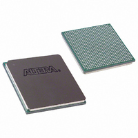
EP2S130F780C5N Altera, EP2S130F780C5N Datasheet - Page 62

EP2S130F780C5N
Manufacturer Part Number
EP2S130F780C5N
Description
IC STRATIX II FPGA 130K 780-FBGA
Manufacturer
Altera
Series
Stratix® IIr
Datasheet
1.EP2S15F484I4N.pdf
(238 pages)
Specifications of EP2S130F780C5N
Number Of Logic Elements/cells
132540
Number Of Labs/clbs
6627
Total Ram Bits
6747840
Number Of I /o
534
Voltage - Supply
1.15 V ~ 1.25 V
Mounting Type
Surface Mount
Operating Temperature
0°C ~ 85°C
Package / Case
780-FBGA
Family Name
Stratix II
Number Of Logic Blocks/elements
132540
# I/os (max)
534
Frequency (max)
609.76MHz
Process Technology
90nm (CMOS)
Operating Supply Voltage (typ)
1.2V
Logic Cells
132540
Ram Bits
6747840
Operating Supply Voltage (min)
1.15V
Operating Supply Voltage (max)
1.25V
Operating Temp Range
0C to 85C
Operating Temperature Classification
Commercial
Mounting
Surface Mount
Pin Count
780
Package Type
FC-FBGA
Lead Free Status / RoHS Status
Lead free / RoHS Compliant
Number Of Gates
-
Lead Free Status / Rohs Status
Compliant
Available stocks
Company
Part Number
Manufacturer
Quantity
Price
Company:
Part Number:
EP2S130F780C5N
Manufacturer:
ALTERA
Quantity:
591
- Current page: 62 of 238
- Download datasheet (3Mb)
PLLs & Clock Networks
2–54
Stratix II Device Handbook, Volume 1
1
Figures 2–37
clock, regional clock, and PLL external clock output, respectively.
Figure 2–37. Global Clock Control Blocks
Notes to
(1)
(2)
These clock select signals can be dynamically controlled through internal logic
when the device is operating in user mode.
These clock select signals can only be set through a configuration file (.sof or .pof)
and cannot be dynamically controlled during user mode operation.
Figure
CLKSELECT[1..0]
When using the global or regional clock control blocks in
Stratix II devices to select between multiple clocks or to enable
and disable clock networks, be aware of possible narrow pulses
or glitches when switching from one clock signal to another. A
glitch or runt pulse has a width that is less than the width of the
highest frequency input clock signal. To prevent logic errors
within the FPGA, Altera recommends that you build circuits
that filter out glitches and runt pulses.
(1)
This multiplexer supports
User-Controllable
Dynamic Switching
through
PLL Counter
2–37:
Outputs
2–39
2
2
show the clock control block for the global
CLKp
Pins
2
Enable/
Disable
GCLK
CLKn
Pin
Internal
Logic
Internal
Static Clock Select
Logic
Altera Corporation
(2)
May 2007
Related parts for EP2S130F780C5N
Image
Part Number
Description
Manufacturer
Datasheet
Request
R

Part Number:
Description:
CYCLONE II STARTER KIT EP2C20N
Manufacturer:
Altera
Datasheet:

Part Number:
Description:
CPLD, EP610 Family, ECMOS Process, 300 Gates, 16 Macro Cells, 16 Reg., 16 User I/Os, 5V Supply, 35 Speed Grade, 24DIP
Manufacturer:
Altera Corporation
Datasheet:

Part Number:
Description:
CPLD, EP610 Family, ECMOS Process, 300 Gates, 16 Macro Cells, 16 Reg., 16 User I/Os, 5V Supply, 15 Speed Grade, 24DIP
Manufacturer:
Altera Corporation
Datasheet:

Part Number:
Description:
Manufacturer:
Altera Corporation
Datasheet:

Part Number:
Description:
CPLD, EP610 Family, ECMOS Process, 300 Gates, 16 Macro Cells, 16 Reg., 16 User I/Os, 5V Supply, 30 Speed Grade, 24DIP
Manufacturer:
Altera Corporation
Datasheet:

Part Number:
Description:
High-performance, low-power erasable programmable logic devices with 8 macrocells, 10ns
Manufacturer:
Altera Corporation
Datasheet:

Part Number:
Description:
High-performance, low-power erasable programmable logic devices with 8 macrocells, 7ns
Manufacturer:
Altera Corporation
Datasheet:

Part Number:
Description:
Classic EPLD
Manufacturer:
Altera Corporation
Datasheet:

Part Number:
Description:
High-performance, low-power erasable programmable logic devices with 8 macrocells, 10ns
Manufacturer:
Altera Corporation
Datasheet:

Part Number:
Description:
Manufacturer:
Altera Corporation
Datasheet:

Part Number:
Description:
Manufacturer:
Altera Corporation
Datasheet:

Part Number:
Description:
Manufacturer:
Altera Corporation
Datasheet:

Part Number:
Description:
CPLD, EP610 Family, ECMOS Process, 300 Gates, 16 Macro Cells, 16 Reg., 16 User I/Os, 5V Supply, 25 Speed Grade, 24DIP
Manufacturer:
Altera Corporation
Datasheet:


