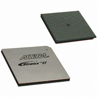
EP2S180F1508C4N Altera, EP2S180F1508C4N Datasheet - Page 209

EP2S180F1508C4N
Manufacturer Part Number
EP2S180F1508C4N
Description
IC STRATIX II FPGA 180K 1508FBGA
Manufacturer
Altera
Series
Stratix® IIr
Datasheet
1.EP2S15F484I4N.pdf
(238 pages)
Specifications of EP2S180F1508C4N
Number Of Logic Elements/cells
179400
Number Of Labs/clbs
8970
Total Ram Bits
9383040
Number Of I /o
1170
Voltage - Supply
1.15 V ~ 1.25 V
Mounting Type
Surface Mount
Operating Temperature
0°C ~ 85°C
Package / Case
1508-FBGA
Family Name
Stratix II
Number Of Logic Blocks/elements
179400
# I/os (max)
1170
Frequency (max)
711.24MHz
Process Technology
90nm (CMOS)
Operating Supply Voltage (typ)
1.2V
Logic Cells
179400
Ram Bits
9383040
Operating Supply Voltage (min)
1.15V
Operating Supply Voltage (max)
1.25V
Operating Temp Range
0C to 85C
Operating Temperature Classification
Commercial
Mounting
Surface Mount
Pin Count
1508
Package Type
FC-FBGA
For Use With
544-1701 - DSP PRO KIT W/SII EP2S180N
Lead Free Status / RoHS Status
Lead free / RoHS Compliant
Number Of Gates
-
Lead Free Status / Rohs Status
Compliant
Other names
544-1887
EP2S180F1508C4N
EP2S180F1508C4N
Available stocks
Company
Part Number
Manufacturer
Quantity
Price
Company:
Part Number:
EP2S180F1508C4N
Manufacturer:
ALTERA
Quantity:
3 000
Part Number:
EP2S180F1508C4N
Manufacturer:
ALTERA/阿尔特拉
Quantity:
20 000
- Current page: 209 of 238
- Download datasheet (3Mb)
Altera Corporation
April 2011
Notes to
(1)
(2)
(3)
(4)
(5)
(6)
1.2-V Differential
HSTL
3.3-V LVTTL
3.3-V LVCMOS
2.5-V
LVTTL/LVCMOS
Table 5–78. Maximum Output Toggle Rate on Stratix II Devices (Part 5 of 5)
Table 5–79. Maximum Output Clock Toggle Rate Derating Factors (Part 1 of 5)
I/O Standard
I/O Standard
The toggle rate applies to 0-pF output load for all I/O standards except for LVDS and HyperTransport technology
on row I/O pins. For LVDS and HyperTransport technology on row I/O pins, the toggle rates apply to load from
0 to 5pF.
1.2-V HSTL is only supported on column I/O pins in I/O banks 4, 7, and 8.
Differential HSTL and SSTL is only supported on column clock and DQS outputs.
HyperTransport technology is only supported on row I/O and row dedicated clock input pins.
LVPECL is only supported on column clock pins.
Refer to
for PLL output.
Table
Tables 5–81
5–78:
Strength
OCT 50 Ω
12 mA
16 mA
20 mA
24 mA
12 mA
16 mA
20 mA
24 mA
12 mA
16 mA
Strength
Drive
4 mA
8 mA
4 mA
8 mA
4 mA
8 mA
Drive
through
5–91
478
260
213
136
138
134
377
206
141
108
387
163
142
120
83
65
-3
Column I/O Pins (MHz)
280
-3
Column I/O Pins
if using SERDES block. Use the toggle rate values from the clock output column
Maximum Output Clock Toggle Rate Derating Factors (ps/pF)
510
333
247
197
187
177
391
212
145
111
427
224
203
182
88
72
-4
-4
-
510
333
247
197
187
177
391
212
145
111
427
224
203
182
88
72
-5
-5
-
478
260
213
377
206
387
163
142
-3
-
-
-
-
-
-
-
-
Row I/O Pins (MHz)
Row I/O Pins
-3
-
510
333
247
391
212
427
224
203
-4
-
-
-
-
-
-
-
-
Stratix II Device Handbook, Volume 1
-4
-
DC & Switching Characteristics
510
333
247
391
212
427
224
203
-5
-
-
-
-
-
-
-
-
-5
-
Note (1)
Dedicated Clock Outputs
466
291
211
166
154
143
377
178
115
391
170
152
134
86
79
74
-3
Clock Outputs (MHz)
280
-3
510
333
247
197
187
177
391
212
145
111
427
224
203
182
88
72
-4
-4
-
510
333
247
197
187
177
391
212
145
111
427
224
203
182
88
72
-5
-5
5–73
-
Related parts for EP2S180F1508C4N
Image
Part Number
Description
Manufacturer
Datasheet
Request
R

Part Number:
Description:
CYCLONE II STARTER KIT EP2C20N
Manufacturer:
Altera
Datasheet:

Part Number:
Description:
CPLD, EP610 Family, ECMOS Process, 300 Gates, 16 Macro Cells, 16 Reg., 16 User I/Os, 5V Supply, 35 Speed Grade, 24DIP
Manufacturer:
Altera Corporation
Datasheet:

Part Number:
Description:
CPLD, EP610 Family, ECMOS Process, 300 Gates, 16 Macro Cells, 16 Reg., 16 User I/Os, 5V Supply, 15 Speed Grade, 24DIP
Manufacturer:
Altera Corporation
Datasheet:

Part Number:
Description:
Manufacturer:
Altera Corporation
Datasheet:

Part Number:
Description:
CPLD, EP610 Family, ECMOS Process, 300 Gates, 16 Macro Cells, 16 Reg., 16 User I/Os, 5V Supply, 30 Speed Grade, 24DIP
Manufacturer:
Altera Corporation
Datasheet:

Part Number:
Description:
High-performance, low-power erasable programmable logic devices with 8 macrocells, 10ns
Manufacturer:
Altera Corporation
Datasheet:

Part Number:
Description:
High-performance, low-power erasable programmable logic devices with 8 macrocells, 7ns
Manufacturer:
Altera Corporation
Datasheet:

Part Number:
Description:
Classic EPLD
Manufacturer:
Altera Corporation
Datasheet:

Part Number:
Description:
High-performance, low-power erasable programmable logic devices with 8 macrocells, 10ns
Manufacturer:
Altera Corporation
Datasheet:

Part Number:
Description:
Manufacturer:
Altera Corporation
Datasheet:

Part Number:
Description:
Manufacturer:
Altera Corporation
Datasheet:

Part Number:
Description:
Manufacturer:
Altera Corporation
Datasheet:

Part Number:
Description:
CPLD, EP610 Family, ECMOS Process, 300 Gates, 16 Macro Cells, 16 Reg., 16 User I/Os, 5V Supply, 25 Speed Grade, 24DIP
Manufacturer:
Altera Corporation
Datasheet:


