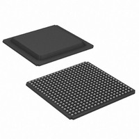
XC3S400AN-4FGG400C Xilinx Inc, XC3S400AN-4FGG400C Datasheet - Page 48

XC3S400AN-4FGG400C
Manufacturer Part Number
XC3S400AN-4FGG400C
Description
IC SPARTAN-3AN FPGA 400K 400FBGA
Manufacturer
Xilinx Inc
Series
Spartan™-3ANr
Datasheets
1.XC3S50A-4VQG100C.pdf
(7 pages)
2.XC3S50AN-4TQG144C.pdf
(2 pages)
3.XC3S50AN-4TQG144C.pdf
(123 pages)
Specifications of XC3S400AN-4FGG400C
Total Ram Bits
368640
Number Of Logic Elements/cells
8064
Number Of Labs/clbs
896
Number Of I /o
311
Number Of Gates
400000
Voltage - Supply
1.14 V ~ 1.26 V
Mounting Type
Surface Mount
Operating Temperature
0°C ~ 85°C
Package / Case
400-BGA
No. Of Logic Blocks
8064
No. Of Gates
400000
No. Of Macrocells
8064
Family Type
Spartan-3AN
No. Of Speed Grades
4
No. Of I/o's
311
Lead Free Status / RoHS Status
Lead free / RoHS Compliant
Other names
122-1554
Available stocks
Company
Part Number
Manufacturer
Quantity
Price
Company:
Part Number:
XC3S400AN-4FGG400C
Manufacturer:
XILINX
Quantity:
3 340
Company:
Part Number:
XC3S400AN-4FGG400C
Manufacturer:
Xilinx Inc
Quantity:
10 000
Part Number:
XC3S400AN-4FGG400C
Manufacturer:
XILINX
Quantity:
20 000
Table 34: CLB Distributed RAM Switching Characteristics
Table 35: CLB Shift Register Switching Characteristics
DS557 (v4.1) April 1, 2011
Product Specification
Notes:
1.
Notes:
1.
Clock-to-Output Times
Setup Times
Hold Times
Clock Pulse Width
Clock-to-Output Times
Setup Times
Hold Times
Clock Pulse Width
T
T
The numbers in this table are based on the operating conditions set forth in
The numbers in this table are based on the operating conditions set forth in
WPH
WPH
T
Symbol
Symbol
T
T
T
AH,
T
SHCKO
SRLDH
SRLDS
T
T
T
T
REG
WS
DS
AS
DH
, T
, T
T
WH
WPL
WPL
Time from the active edge at the CLK input to data appearing on
the distributed RAM output
Setup time of data at the BX or BY input before the active
transition at the CLK input of the distributed RAM
Setup time of the F/G address inputs before the active transition
at the CLK input of the distributed RAM
Setup time of the write enable input before the active transition at
the CLK input of the distributed RAM
Hold time of the BX and BY data inputs after the active transition
at the CLK input of the distributed RAM
Hold time of the F/G address inputs or the write enable input after
the active transition at the CLK input of the distributed RAM
Minimum High or Low pulse width at CLK input
Time from the active edge at the CLK input to data appearing on
the shift register output
Setup time of data at the BX or BY input before the active
transition at the CLK input of the shift register
Hold time of the BX or BY data input after the active transition at
the CLK input of the shift register
Minimum High or Low pulse width at CLK input
Description
Description
www.xilinx.com
Spartan-3AN FPGA Family: DC and Switching Characteristics
Table
Table
10.
10.
–0.07
0.18
0.30
0.13
0.01
0.88
0.13
0.16
0.90
Min
Min
–
–
-5
-5
Speed Grade
Speed Grade
Max
1.69
Max
4.11
–
–
–
–
–
–
–
–
–
–0.02
0.36
0.59
0.13
0.01
1.01
0.18
0.16
1.01
Min
Min
–
–
-4
-4
Max
Max
2.01
4.82
–
–
–
–
–
–
–
–
–
Units
Units
ns
ns
ns
ns
ns
ns
ns
ns
ns
ns
ns
48


