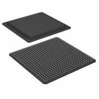
XCV405E-7FG676I Xilinx Inc, XCV405E-7FG676I Datasheet - Page 23

XCV405E-7FG676I
Manufacturer Part Number
XCV405E-7FG676I
Description
IC FPGA 1.8V 676-BGA
Manufacturer
Xilinx Inc
Series
Virtex™-E EMr
Datasheet
1.XCV405E-6FG676C.pdf
(118 pages)
Specifications of XCV405E-7FG676I
Number Of Logic Elements/cells
10800
Number Of Labs/clbs
2400
Total Ram Bits
573440
Number Of I /o
404
Number Of Gates
129600
Voltage - Supply
1.71 V ~ 1.89 V
Mounting Type
Surface Mount
Operating Temperature
-40°C ~ 100°C
Package / Case
676-BBGA
Lead Free Status / RoHS Status
Contains lead / RoHS non-compliant
Available stocks
Company
Part Number
Manufacturer
Quantity
Price
Company:
Part Number:
XCV405E-7FG676I
Manufacturer:
XilinxInc
Quantity:
3 000
Part Number:
XCV405E-7FG676I
Manufacturer:
XILINX/赛灵思
Quantity:
20 000
the internal storage elements to begin changing state in
response to the logic and the user clock.
The relative timing of these events can be changed. In addi-
tion, the GTS, GSR, and GWE events can be made depen-
Readback
The configuration data stored in the Virtex-E configuration
memory can be readback for verification. Along with the
configuration data it is possible to readback the contents all
flip-flops/latches, LUT RAMs, and block RAMs. This capa-
DS025-2 (v2.3) November 19, 2002
R
Virtex™-E 1.8 V Extended Memory Field Programmable Gate Arrays
www.xilinx.com
1-800-255-7778
dent on the DONE pins of multiple devices all going High,
forcing the devices to start synchronously. The sequence
can also be paused at any stage until lock has been
achieved on any or all DLLs.
bility is used for real-time debugging. For more detailed
information, see application note XAPP138 “Virtex FPGA
Series Configuration and Readback”.
Module 2 of 4
19


