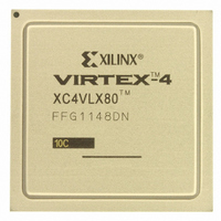
XC4VLX80-10FFG1148C Xilinx Inc, XC4VLX80-10FFG1148C Datasheet - Page 44

XC4VLX80-10FFG1148C
Manufacturer Part Number
XC4VLX80-10FFG1148C
Description
IC FPGA VIRTEX-4 80K 1148-FBGA
Manufacturer
Xilinx Inc
Series
Virtex™-4r
Specifications of XC4VLX80-10FFG1148C
Total Ram Bits
3686400
Number Of Logic Elements/cells
80640
Number Of Labs/clbs
8960
Number Of I /o
768
Voltage - Supply
1.14 V ~ 1.26 V
Mounting Type
Surface Mount
Operating Temperature
0°C ~ 85°C
Package / Case
1148-BBGA, FCBGA
No. Of Logic Blocks
8960
No. Of Macrocells
80640
Family Type
Virtex-4
No. Of Speed Grades
10
No. Of I/o's
768
Clock Management
DCM
Core Supply
RoHS Compliant
Lead Free Status / RoHS Status
Lead free / RoHS Compliant
Number Of Gates
-
Lead Free Status / RoHS Status
Lead free / RoHS Compliant
Other names
122-1497
Available stocks
Company
Part Number
Manufacturer
Quantity
Price
Company:
Part Number:
XC4VLX80-10FFG1148C
Manufacturer:
XILINX
Quantity:
120
Company:
Part Number:
XC4VLX80-10FFG1148C
Manufacturer:
Xilinx Inc
Quantity:
10 000
Part Number:
XC4VLX80-10FFG1148C
Manufacturer:
XILINX/赛灵思
Quantity:
20 000
System-Synchronous Switching Characteristics
Virtex-4 FPGA Pin-to-Pin Output Parameter Guidelines
All devices are 100% functionally tested. The representative values for typical pin locations and normal clock loading are
listed in
Table 54: Global Clock Input to Output Delay for LVCMOS25 Standard, 12 mA, Fast Slew Rate, with DCM
DS302 (v3.7) September 9, 2009
Product Specification
Notes:
1.
2.
LVCMOS25 Global Clock Input to Output Delay using Output Flip-Flop, 12mA, Fast Slew Rate, with DCM.
T
ICKOFDCM
Listed above are representative values where one global clock input drives one vertical clock line in each accessible column, and where all
accessible IOB and CLB flip-flops are clocked by the global clock net.
DCM output jitter is already included in the timing calculation.
Symbol
Table
54. Values are expressed in nanoseconds unless otherwise noted.
Global Clock and OFF with DCM
Description
www.xilinx.com
Virtex-4 FPGA Data Sheet: DC and Switching Characteristics
XC4VFX100
XC4VFX140
XC4VLX100
XC4VLX160
XC4VLX200
XC4VSX25
XC4VSX35
XC4VSX55
XC4VFX12
XC4VFX20
XC4VFX40
XC4VFX60
XC4VLX15
XC4VLX25
XC4VLX40
XC4VLX60
XC4VLX80
Device
2.43
2.60
2.54
2.69
2.88
2.94
2.94
2.65
2.81
2.83
2.43
2.54
2.87
2.92
3.16
N/A
N/A
-12
Speed Grade
2.81
2.95
2.91
3.05
3.27
3.33
3.35
3.51
2.99
3.18
3.20
2.78
2.88
3.25
3.31
3.58
3.79
-11
3.25
3.36
3.32
3.45
3.72
3.79
3.82
4.02
3.39
3.60
3.62
3.18
3.26
3.67
3.77
4.06
4.30
-10
Units
ns
ns
ns
ns
ns
ns
ns
ns
ns
ns
ns
ns
ns
ns
ns
ns
ns
44


