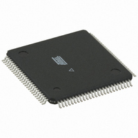
AT94K05AL-25AQU Atmel, AT94K05AL-25AQU Datasheet - Page 104

AT94K05AL-25AQU
Manufacturer Part Number
AT94K05AL-25AQU
Description
IC FPSLIC 5K GATE 25MHZ 100-TQFP
Manufacturer
Atmel
Series
FPSLIC®r
Datasheet
1.AT94K05AL-25AJI.pdf
(204 pages)
Specifications of AT94K05AL-25AQU
Core Type
8-bit AVR
Speed
25MHz
Interface
I²C, UART
Program Sram Bytes
4K-16K
Fpga Sram
2kb
Data Sram Bytes
4K ~ 16K
Fpga Core Cells
256
Fpga Gates
5K
Fpga Registers
436
Voltage - Supply
3 V ~ 3.6 V
Mounting Type
Surface Mount
Operating Temperature
-40°C ~ 85°C
Package / Case
100-TQFP, 100-VQFP
For Use With
ATSTK594 - BOARD FPSLIC DAUGHTER FOR STK500
Lead Free Status / RoHS Status
Lead free / RoHS Compliant
Eeprom Size
-
Available stocks
Company
Part Number
Manufacturer
Quantity
Price
- Current page: 104 of 204
- Download datasheet (4Mb)
104
AT94KAL Series FPSLIC
Timer/Counter1 Control Register B – TCCR1B
• Bit 7 - ICNC1: Input Capture1 Noise Canceler (4 CKs)
When the ICNC1 bit is cleared (zero), the input capture trigger noise canceler function is dis-
abled. The input capture is triggered at the first rising/falling edge sampled on the PE7(ICP) –
input capture pin – as specified. When the ICNC1 bit is set (one), four successive samples are
measured on the PE7(ICP) – input capture pin, and all samples must be High/Low according to
the input capture trigger specification in the ICES1 bit. The actual sampling frequency is XTAL
clock frequency.
• Bit 6 - ICES1: Input Capture1 Edge Select
While the ICES1 bit is cleared (zero), the Timer/Counter1 contents are transferred to the Input
Capture Register – ICR1 – on the falling edge of the input capture pin – PE7(ICP). While the
ICES1 bit is set (one), the Timer/Counter1 contents are transferred to the Input Capture Register
– ICR1 – on the rising edge of the input capture pin – PE7(ICP).
• Bit 5 - ICPE: Input Captive Pin Enable
This bit must be set by the user to enable the Input Capture Function of timer1. Disabling pre-
vents unnecessary register copies during normal use of the PE7 port.
• Bit 4 - Res: Reserved Bit
This bit is reserved in the FPSLIC and will always read zero.
• Bit 3 - CTC1: Clear Timer/Counter1 on Compare Match
When the CTC1 control bit is set (one), the Timer/Counter1 is reset to $0000 in the clock cycle
after a compareA match. If the CTC1 control bit is cleared, Timer/Counter1 continues counting
and is unaffected by a compare match. When a prescaling of 1 is used, and the compareA reg-
ister is set to C, the timer will count as follows if CTC1 is set:
... | C-1 | C | 0 | 1 | ...
When the prescaler is set to divide by 8, the timer will count like this:
... | C-1, C-1, C-1, C-1, C-1, C-1, C-1, C-1 | C, C, C, C, C, C, C, C | 0, 0, 0, 0, 0, 0, 0, 0 | ...
In PWM mode, this bit has a different function. If the CTC1 bit is cleared in PWM mode, the
Timer/Counter1 acts as an up/down counter. If the CTC1 bit is set (one), the Timer/Counter
wraps when it reaches the TOP value. Refer to
• Bits 2,1,0 - CS12, CS11, CS10: Clock Select1, Bits 2, 1 and 0
The Clock Select1 bits 2,1 and 0 define the prescaling source of Timer/Counter1.
Bit
$2E ($4E)
Read/Write
Initial Value
7
ICNC1
R/W
0
6
ICES1
R/W
0
5
ICPE
0
R/W
4
-
R
0
page 107
3
CTC1
R/W
0
for a detailed description.
2
CS12
R/W
0
1
CS11
0
R/W
0
CS10
R/W
0
1138I–FPSLI–1/08
TCCR1B
Related parts for AT94K05AL-25AQU
Image
Part Number
Description
Manufacturer
Datasheet
Request
R

Part Number:
Description:
IC FPSLIC 5K GATE 25MHZ 84PLCC
Manufacturer:
Atmel
Datasheet:

Part Number:
Description:
Fpslic Devices Combine 5K Gates of Atmel's Patented AT40K Fpga Architecture, a 20 Mips Avr 8-bit Risc Microprocessor Core, Numerous Fixed Microcontroller Peripheries And up to 36K Bytes of Program And Data SRAM.
Manufacturer:
ATMEL Corporation
Datasheet:

Part Number:
Description:
IC FPSLIC 5K GATE 25MHZ 84PLCC
Manufacturer:
Atmel
Datasheet:

Part Number:
Description:
IC FPSLIC 5K GATE 25MHZ 208PQFP
Manufacturer:
Atmel
Datasheet:

Part Number:
Description:
IC FPSLIC 5K GATE 25MHZ 144LQFP
Manufacturer:
Atmel
Datasheet:

Part Number:
Description:
IC FPSLIC 5K GATE 25MHZ 208PQFP
Manufacturer:
Atmel
Datasheet:

Part Number:
Description:
IC FPSLIC 5K GATE 25MHZ 144LQFP
Manufacturer:
Atmel
Datasheet:

Part Number:
Description:
IC FPSLIC 5K GATE 25MHZ 144-LQFP
Manufacturer:
Atmel
Datasheet:

Part Number:
Description:
Manufacturer:
Atmel
Datasheet:

Part Number:
Description:
Manufacturer:
Atmel
Datasheet:

Part Number:
Description:
Manufacturer:
Atmel
Datasheet:

Part Number:
Description:
5k - 40k Gates Of At40k Fpga With 8-bit Microcontroller, Up To 36k Bytes Of Sram And On-chip Jtag Ice
Manufacturer:
ATMEL Corporation
Datasheet:

Part Number:
Description:
At94k05al 5k - 40k Gates Of At40k Fpga With 8-bit Microcontroller, Up To 36k Bytes Of Sram And On-chip Jtag Ice
Manufacturer:
ATMEL Corporation
Datasheet:

Part Number:
Description:
DEV KIT FOR AVR/AVR32
Manufacturer:
Atmel
Datasheet:


