DLP-FPGA DLP Design Inc, DLP-FPGA Datasheet - Page 3
DLP-FPGA
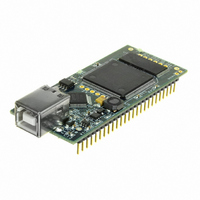
Manufacturer Part Number
DLP-FPGA
Description
MODULE USB-TO-FPGA TRAINING TOOL
Manufacturer
DLP Design Inc
Datasheet
1.DLP-FPGA.pdf
(10 pages)
Specifications of DLP-FPGA
Module/board Type
FPGA Module
Interface Type
USB, SPI
Product
Interface Modules
For Use With/related Products
USB
Lead Free Status / RoHS Status
Lead free / RoHS Compliant
Lead Free Status / RoHS Status
Lead free / RoHS Compliant, Lead free / RoHS Compliant
Other names
813-1008


Chapter 4: Lab 3: Memory Test: Block Diagram, DCM Design, SRAM State Machine, Bi-Directional
Buffers, Test Failed Indicator, User Constraint File, Synthesize the Memory Test Design, Simulate the
Memory Test Design, Implementing the Design, Download the Design to the FPGA
Chapter 5: Lab 4: USB Loopback: Initial Design, USB State Machine Module, Language Template,
Bi-Directional Buffers, Synthesize, Simulate, Pin Constraints, Implement, Download the Design to the
FPGA
(The completed design files for each lab are available for download from the DLP Design website
upon purchase of the DLP-FPGA and Lab Manual.)
3.0 FPGA SPECIFICATIONS
The FPGA device used on the DLP-FPGA is the Xilinx Spartan 3E:
4.0 BITLOADAPP SOFTWARE
Windows software is provided for use with the DLP-FPGA that will load an FPGA configuration (.bit)
file directly to the SPI Flash device via the USB interface. This app (shown below) will allow the user
to erase the flash, verify the erasure and then program and verify the flash:
Rev. 1.4 (November 2010)
•
•
•
•
•
•
•
•
Part Number: XC3S250E
System Gates: 250K
Equivalent Logic Cells: 5,508
CLB Array
Distributed RAM Bits: 38K
Block RAM Bits: 216K
Dedicated Multipliers: 12
DCM’s: 4
o Rows: 34
o Columns: 26
o Total CLB’s: 612
o Total Slices: 2,448
3
XC3S250E-4TQ144
© DLP Design, Inc.
.
Related parts for DLP-FPGA
Image
Part Number
Description
Manufacturer
Datasheet
Request
R

Part Number:
Description:
MODULE USB-MCU FT245RL W/16F877A
Manufacturer:
DLP Design Inc
Datasheet:

Part Number:
Description:
MODULE USB-MCU FT232R W/18F2410
Manufacturer:
DLP Design Inc
Datasheet:

Part Number:
Description:
MODULE USB-MCU FT245RL W/SX48
Manufacturer:
DLP Design Inc
Datasheet:

Part Number:
Description:
MODULE USB-MCU FT2232D W/16F877A
Manufacturer:
DLP Design Inc
Datasheet:

Part Number:
Description:
MODULE USB-TO-FPGA SPARTAN3
Manufacturer:
DLP Design Inc
Datasheet:

Part Number:
Description:
MOD USB-MCU FT245RL W/18LF8722
Manufacturer:
DLP Design Inc
Datasheet:

Part Number:
Description:
Zigbee / 802.15.4 Modules & Development Tools PC INTERFACE HOST MODULE (USB)
Manufacturer:
DLP Design Inc
Datasheet:

Part Number:
Description:
Zigbee / 802.15.4 Modules & Development Tools TTL SERIAL INTERFACE MODULE
Manufacturer:
DLP Design Inc
Datasheet:

Part Number:
Description:
MODULE USB SECURITY DONGLE
Manufacturer:
DLP Design Inc
Datasheet:

Part Number:
Description:
MODULE DATA-ACQUISITION 3-CH
Manufacturer:
DLP Design Inc
Datasheet:

Part Number:
Description:
MODULE LATCHING-RELAY 4-CH
Manufacturer:
DLP Design Inc
Datasheet:

Part Number:
Description:
MODULE USB-TO-TTL SRL UART CONV
Manufacturer:
DLP Design Inc
Datasheet:
Part Number:
Description:
MODULE USB-TO-TTL SRL UART CONV
Manufacturer:
DLP Design Inc
Datasheet:

Part Number:
Description:
MODULE USB-TO-TTL PARL FIFO CONV
Manufacturer:
DLP Design Inc
Datasheet:

Part Number:
Description:
MODULE DATA-ACQUISITION 8-CH
Manufacturer:
DLP Design Inc
Datasheet: