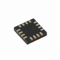
CY8CTMG200-16LGXI Cypress Semiconductor Corp, CY8CTMG200-16LGXI Datasheet - Page 183

CY8CTMG200-16LGXI
Manufacturer Part Number
CY8CTMG200-16LGXI
Description
IC MCU 32K FLASH 16-COL
Manufacturer
Cypress Semiconductor Corp
Series
TrueTouch™r
Datasheet
1.CY8CTST200-16LGXI.pdf
(308 pages)
Specifications of CY8CTMG200-16LGXI
Applications
Touchscreen Controller
Core Processor
M8C
Program Memory Type
FLASH (32 kB)
Controller Series
CY8CT
Ram Size
2K x 8
Interface
I²C, SPI, UART/USART, USB
Number Of I /o
13
Voltage - Supply
1.8 V
Operating Temperature
-40°C ~ 85°C
Mounting Type
Surface Mount
Package / Case
16-QFN
Processor Series
CY8CTxx2xx
Core
M8C
Data Bus Width
8 bit
For Use With
770-1000 - ISP 4PORT FOR CYPRESS PSOC MCU
Lead Free Status / RoHS Status
Lead free / RoHS Compliant
Other names
428-2952
Available stocks
Company
Part Number
Manufacturer
Quantity
Price
Company:
Part Number:
CY8CTMG200-16LGXI
Manufacturer:
CY
Quantity:
490
- Current page: 183 of 308
- Download datasheet (3Mb)
The Registers section discusses the registers of the PSoC device. It lists all the registers in mapping tables, in address order.
For easy reference, each register is linked to the page of a detailed description located in the next chapter. This section
encompasses the following chapter:
■
Register General Conventions
The register conventions specific to this section and the
Register Reference chapter are listed in the following table:
Register Conventions
PSoC CY8CTMG20x and CY8CTST200 TRM, Document No. 001-53603 Rev. *C
Empty, grayed-out
table cell
‘x’ before the comma
in an address
‘x’ in a register name
R
W
O
L
C
#
Section E: Registers
Register Reference chapter on page
Convention
Illustrates a reserved bit or group of bits.
Indicates the register exists in register bank 1 and
register bank 2.
Indicates that there are multiple instances/address
ranges of the same register.
Read register or bit(s).
Write register or bit(s).
Only a read/write register or bit(s).
Logical register or bit(s).
Clearable register or bit(s).
Access is bit specific.
Description
187.
Register Mapping Tables
The PSoC device has a total register address space of 512
bytes. The register space is also referred to as I/O space
and is broken into two parts: Bank 0 (user space) and Bank
1 (configuration space). The XIO bit in the Flag register
(CPU_F) determines which bank the user is currently in.
When the XIO bit is set, the user is said to be in the
“extended” address space or the “configuration” registers.
Refer to the individual PSoC device data sheets for device-
specific register mapping information.
183
[+] Feedback
Related parts for CY8CTMG200-16LGXI
Image
Part Number
Description
Manufacturer
Datasheet
Request
R
Part Number:
Description:
CY8CTMG200-32LQXIT
Manufacturer:
Cypress Semiconductor Corp
Datasheet:

Part Number:
Description:
IC MCU 32K FLASH 24UQFN
Manufacturer:
Cypress Semiconductor Corp
Datasheet:

Part Number:
Description:
IC MCU 32K FLASH 32UQFN
Manufacturer:
Cypress Semiconductor Corp
Datasheet:

Part Number:
Description:
IC MCU 32K FLASH 48-QFN
Manufacturer:
Cypress Semiconductor Corp
Datasheet:
Part Number:
Description:
IC MCU 32K FLASH 16-COL
Manufacturer:
Cypress Semiconductor Corp
Datasheet:
Part Number:
Description:
IC MCU 32K FLASH 24UQFN
Manufacturer:
Cypress Semiconductor Corp
Datasheet:
Part Number:
Description:
IC MCU 32K FLASH 48-QFN
Manufacturer:
Cypress Semiconductor Corp
Datasheet:
Part Number:
Description:
Manufacturer:
Cypress Semiconductor Corp
Datasheet:
Part Number:
Description:
Manufacturer:
Cypress Semiconductor Corp
Datasheet:


