MM908E626AVEK Freescale Semiconductor, MM908E626AVEK Datasheet - Page 32
MM908E626AVEK
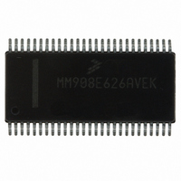
Manufacturer Part Number
MM908E626AVEK
Description
IC STEPPER MOTOR DRIVER 54-SOIC
Manufacturer
Freescale Semiconductor
Type
Stepper Motor Driverr
Datasheet
1.MM908E626AVEK.pdf
(44 pages)
Specifications of MM908E626AVEK
Applications
Automotive Mirror Control
Core Processor
HC08
Program Memory Type
FLASH (16 kB)
Controller Series
908E
Ram Size
512 x 8
Interface
SCI, SPI
Number Of I /o
13
Voltage - Supply
8 V ~ 18 V
Operating Temperature
-40°C ~ 115°C
Mounting Type
Surface Mount
Package / Case
54-SOIC (7.5mm Width) Exposed Pad, 54-eSOIC, 54-HSOIC
Product
Stepper Motor Controllers / Drivers
Supply Current
20 mA
Lead Free Status / RoHS Status
Lead free / RoHS Compliant
Available stocks
Company
Part Number
Manufacturer
Quantity
Price

Part Number:
MM908E626AVEK
Manufacturer:
FREESCALE
Quantity:
20 000


AWDR — Autonomous Watchdog Rate Bit
Autonomous Watchdog. Reset clears the AWDR bit.
VOLTAGE REGULATOR
regulator to provide internal power and external power for the
MCU. The V
and provides a regulated V
the device. The output of the regulator is also connected to
the VDD pin to provide the 5.0V to the microcontroller.
V
parameters (e.g. ICG trim value) are stored in the flash
memory of the device. The following flash memory locations
are reserved for this purpose and might have a value different
from the empty (0xFF) state:
has to take care not to erase or override these values. If these
parameters are not used, these flash locations can be erased
and otherwise used.
Trim Values
memory is explained
32
908E626
FUNCTIONAL DEVICE OPERATION
FACTORY TRIMMING AND CALIBRATION
DD
This read / write bit selects the clock rate of the
• 1 = Fast rate selected (10ms).
• 0 = Slow rate selected (20ms).
The 908E626 chip contains a low power, low drop voltage
Note: Under loss of power conditions, the discharge of the
To enhance the ease-of-use of the 908E626, various
• 0xFD80: 0xFDDF Trim and Calibration Values
• 0xFFFE : 0xFFFF Reset Vector
In the event the application uses these parameters, one
Below the usage of the trim values located in the flash
capacitor may occur relatively slow. Based on the
DD
regulator accepts a unregulated input supply
DD
supply to all digital sections of
FACTORY TRIMMING AND CALIBRATION
selected external components and external V
additional external load may be required guarantee the MCU
POR threshold being reached before the next power up.
RUN Mode
provides a regulated supply to all digital sections.
STOP Mode
regulated output voltage. The STOP mode regulator has a
very limited output current capability. The output voltage will
be lower than the output voltage of the main voltage
regulator.
Internal Clock Generator (ICG) Trim Value
create a stable clock source for the microcontroller without
using any external components. The untrimmed frequency of
the low frequency base clock (IBASE), will vary as much as
±25 percent due to process, temperature, and voltage
dependencies. To compensate this dependencies a ICG trim
values is located at address $FDC2. After trimming the ICG
is a range of typ. ±2% (±3% max.) at nominal conditions
(filtered (100nF) and stabilized (4.7uF) V
T
(VDD) as indicated in the 68HC908EY16 datasheet.
Trim Register ICGTR at address $38 of the MCU.
Ambient
During RUN mode, the main voltage regulator is on. It
During STOP mode the STOP mode regulator supplies a
The internal clock generator (ICG) module is used to
To trim the ICG this values has to be copied to the ICG
Important The value has to be copied after every reset.
~25°C) and will vary over temperature and voltage
Analog Integrated Circuit Device Data
Freescale Semiconductor
DD
= 5V,
DD
load,
Related parts for MM908E626AVEK
Image
Part Number
Description
Manufacturer
Datasheet
Request
R

Part Number:
Description:
Manufacturer:
Freescale Semiconductor, Inc
Datasheet:
Part Number:
Description:
Manufacturer:
Freescale Semiconductor, Inc
Datasheet:
Part Number:
Description:
Manufacturer:
Freescale Semiconductor, Inc
Datasheet:
Part Number:
Description:
Manufacturer:
Freescale Semiconductor, Inc
Datasheet:
Part Number:
Description:
Manufacturer:
Freescale Semiconductor, Inc
Datasheet:
Part Number:
Description:
Manufacturer:
Freescale Semiconductor, Inc
Datasheet:
Part Number:
Description:
Manufacturer:
Freescale Semiconductor, Inc
Datasheet:
Part Number:
Description:
Manufacturer:
Freescale Semiconductor, Inc
Datasheet:
Part Number:
Description:
Manufacturer:
Freescale Semiconductor, Inc
Datasheet:
Part Number:
Description:
Manufacturer:
Freescale Semiconductor, Inc
Datasheet:
Part Number:
Description:
Manufacturer:
Freescale Semiconductor, Inc
Datasheet:
Part Number:
Description:
Manufacturer:
Freescale Semiconductor, Inc
Datasheet:
Part Number:
Description:
Manufacturer:
Freescale Semiconductor, Inc
Datasheet:
Part Number:
Description:
Manufacturer:
Freescale Semiconductor, Inc
Datasheet:
Part Number:
Description:
Manufacturer:
Freescale Semiconductor, Inc
Datasheet: