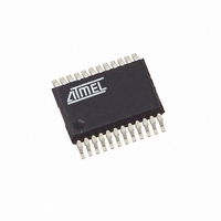
ATAM862P-TNSY3D Atmel, ATAM862P-TNSY3D Datasheet - Page 32

ATAM862P-TNSY3D
Manufacturer Part Number
ATAM862P-TNSY3D
Description
IC MCU FLASH 4K TX 315MHZ 24SSOP
Manufacturer
Atmel
Datasheet
1.ATAM862P-TNQY3D.pdf
(110 pages)
Specifications of ATAM862P-TNSY3D
Applications
UHF ASK/FSK
Core Processor
MARC4
Program Memory Type
FLASH (4 kB)
Controller Series
MARC4 4-Bit
Ram Size
256 x 4
Interface
SSI
Number Of I /o
11
Voltage - Supply
1.8 V ~ 4 V
Operating Temperature
-40°C ~ 125°C
Mounting Type
Surface Mount
Package / Case
24-SSOP
Processor Series
ATAM862x
Core
MARC4
Data Bus Width
4 bit
Mounting Style
SMD/SMT
Lead Free Status / RoHS Status
Lead free / RoHS Compliant
21. Peripheral Modules
21.1
32
Addressing Peripherals
ATAM862-3
The microcontroller block has various power-down modes. During the sleep mode the clock for
the microcontroller block core is stopped. With the NSTOP bit in the clock management register
(CM), it is programmable if the clock for the on-chip peripherals is active or stopped during the
sleep mode. If the clock for the core and the peripherals is stopped, the selected oscillator is
switched off. An exception is the 32-kHz oscillator, if it is selected it runs continuously indepen-
dent of the NSTOP bit. If the oscillator is stopped or the 32-kHz oscillator is selected, power
consumption is extremely low.
Table 20-1.
Accessing the peripheral modules takes place via the I/O bus (see
33). The IN or OUT instructions allow direct addressing of up to 16 I/O modules. A dual register
addressing scheme has been adopted to enable direct addressing of the primary register. To
address the auxiliary register, the access must be switched with an auxiliary switching module.
Thus, a single IN (or OUT) to the module address will read (or write into) the module primary
register. Accessing the auxiliary register is performed with the same instruction preceded by
writing the module address into the auxiliary switching module. Byte wide registers are accessed
by multiple IN- (or OUT-) instructions. For more complex peripheral modules, with a larger num-
ber of registers, extended addressing is used. In this case, a bank of up to 16 subport registers
are indirectly addressed with the subport address. The first OUT instruction writes the subport
address to the sub address register, the second IN or OUT instruction reads data from or writes
data to the addressed subport.
Note:
Power-down
SLEEP
Mode
Active
1. Osc-Stop = SLEEP and NSTOP and WDL
Power-down Mode
CPU Core
SLEEP
SLEEP
RUN
Osc-Stop
YES
NO
NO
1)
(
Brown-out
Function
Active
Active
STOP
4-MHz Oscillator
RC-oscillator 1
RC-oscillator 2
STOP
RUN
RUN
Oscillator
32-kHz
RUN
RUN
RUN
Figure 21-1 on page
4554F–4BMCU–07/07
Input Clock
External
STOP
YES
YES


