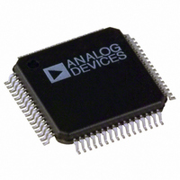
ADE7566ASTZF8 Analog Devices Inc, ADE7566ASTZF8 Datasheet - Page 70

ADE7566ASTZF8
Manufacturer Part Number
ADE7566ASTZF8
Description
IC ENERGY METER MCU 8K 64LQFP
Manufacturer
Analog Devices Inc
Datasheets
1.ADE7169ASTZF16.pdf
(152 pages)
2.ADE7566ASTZF8-RL.pdf
(136 pages)
3.ADE7169ASTZF16.pdf
(144 pages)
Specifications of ADE7566ASTZF8
Applications
Energy Measurement
Core Processor
8052
Program Memory Type
FLASH (8 kB)
Controller Series
ADE75xx
Ram Size
512 x 8
Interface
I²C, SPI, UART
Number Of I /o
20
Voltage - Supply
3.135 V ~ 3.465 V
Operating Temperature
-40°C ~ 85°C
Mounting Type
Surface Mount
Package / Case
64-LQFP
Ic Function
Single Phase Energy Measurement IC
Supply Voltage Range
3.13V To 3.46V, 2.4V To 3.7V
Operating Temperature Range
-40°C To +85°C
Digital Ic Case Style
LQFP
No. Of Pins
64
Lead Free Status / RoHS Status
Lead free / RoHS Compliant
Available stocks
Company
Part Number
Manufacturer
Quantity
Price
Company:
Part Number:
ADE7566ASTZF8
Manufacturer:
Analog Devices Inc
Quantity:
10 000
Company:
Part Number:
ADE7566ASTZF8-RL
Manufacturer:
Analog Devices Inc
Quantity:
10 000
ADE7566/ADE7569
8052 MCU CORE ARCHITECTURE
The ADE7566/ADE7569 have an 8052 MCU core and use the
8051 instruction set. Some of the standard 8052 peripherals,
such as the UART, have been enhanced. This section describes
the standard 8052 core and its enhancements used in the
ADE7566/ADE7569.
The special function register (SFR) space is mapped into the
upper 128 bytes of internal data memory space and is accessed
by direct addressing only. It provides an interface between the
CPU and all on-chip peripherals. A block diagram showing the
programming model of the ADE7566/ADE7569 via the SFR
area is shown in Figure 67.
All registers except the program counter (PC), instruction
register (IR), and the four general-purpose register banks
reside in the SFR area. The SFR registers include power
control, configuration, and data registers that provide an
interface between the CPU and all on-chip peripherals.
MCU REGISTERS
The registers used by the MCU are summarized in this section.
Table 52. 8051 SFRs
SFR
A
B
PSW
PCON
DPL
DPH
DPTR
SP
CFG
Table 53. Program Status Word SFR (PSW, 0xD0)
Bit No.
7
6
5
4 to 3
2
1
0
Address
0xD7
0xD6
0xD5
0xD4, 0xD3
0xD2
0xD1
0xD0
Address
0xE0
0xF0
0xD0
0x87
0x82
0x83
0x83 and 0x82
0x81
0xAF
Mnemonic
CY
AC
F0
RS1, RS0
OV
F1
P
Bit Addressable
Yes
Yes
Yes
No
No
No
No
No
No
Description
Carry Flag. Modified by ADD, ADDC, SUBB, MUL, and DIV instructions.
Auxiliary Carry Flag. Modified by ADD and ADDC instructions.
General-Purpose Flag Available to the User.
Register Bank Select Bits.
RS1
0
0
1
1
Overflow Flag. Modified by ADD, ADDC, SUBB, MUL, and DIV instructions.
General-Purpose Flag Available to the User.
Parity Bit. The number of bits set in the accumulator added to the value of the parity bit is always an
even number.
RS0
0
1
0
1
Result (Selected Bank)
0
1
2
3
Rev. PrA | Page 70 of 136
Description
Accumulator.
Auxiliary Math Register.
Program Status Word (see Table 53).
Power Control Register (see Table 54).
Data Pointer LSByte (see Table 55).
Data Pointer MSByte (see Table 56).
16-Bit Data Pointer (see Table 57).
Stack Pointer LSByte (see Table 58).
Configuration (see Table 59).
256 BYTES
REGISTER
GENERAL
PURPOSE
BANKS
STACK
RAM
Figure 67. ADE7566/ADE7569 Block Diagram
16kB ELECTRICALLY
REPROGRAMMABLE
PROGRAM/DATA
256 BYTES XRAM
NONVOLATILE
COMPATIBLE
PC
FLASH/EE
MEMORY
Preliminary Technical Data
CORE
8051
IR
FUNCTION
REGISTER
128-BYTE
SPECIAL
AREA
OTHER ON-CHIP
PERIPHERALS:
SERIAL I/O
WDT
TIMERS
MEASUREMENT
TEMPERATURE
MANAGEMENT
LCD DRIVER
BATTERY
ENERGY
POWER
RTC
ADC
ADC


