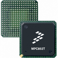
MPC852TCVR50A Freescale Semiconductor, MPC852TCVR50A Datasheet - Page 35

MPC852TCVR50A
Manufacturer Part Number
MPC852TCVR50A
Description
IC MPU POWERQUICC 50MHZ 256PBGA
Manufacturer
Freescale Semiconductor
Series
PowerQUICC Ir
Datasheet
1.MPC852TVR50A.pdf
(80 pages)
Specifications of MPC852TCVR50A
Processor Type
MPC8xx PowerQUICC 32-Bit
Speed
50MHz
Voltage
1.8V
Mounting Type
Surface Mount
Package / Case
256-PBGA
Family Name
MPC8xx
Device Core
PowerQUICC
Device Core Size
32b
Frequency (max)
50MHz
Instruction Set Architecture
RISC
Supply Voltage 1 (typ)
1.8/3.3V
Operating Supply Voltage (max)
1.9/3.465V
Operating Supply Voltage (min)
1.7/3.135V
Operating Temp Range
-40C to 100C
Operating Temperature Classification
Industrial
Mounting
Surface Mount
Pin Count
256
Package Type
BGA
Core Size
32 Bit
Program Memory Size
8KB
Cpu Speed
50MHz
Embedded Interface Type
SPI, UART
Digital Ic Case Style
BGA
No. Of Pins
256
Supply Voltage Range
1.7V To 1.9V
Rohs Compliant
Yes
Lead Free Status / RoHS Status
Lead free / RoHS Compliant
Features
-
Lead Free Status / Rohs Status
Compliant
Available stocks
Company
Part Number
Manufacturer
Quantity
Price
Company:
Part Number:
MPC852TCVR50A
Manufacturer:
Freescale
Quantity:
486
Company:
Part Number:
MPC852TCVR50A
Manufacturer:
MOTOROLA
Quantity:
325
Company:
Part Number:
MPC852TCVR50A
Manufacturer:
Freescale Semiconductor
Quantity:
10 000
Table 11
1
These synchronous timings define when the WAITA signals are detected in order to freeze (or relieve) the
PCMCIA current cycle. The WAITA assertion is effective only if it is detected 2 cycles before the PSL
timer expiration. See the PCMCIA Interface section in the MPC866 PowerQUICC™ Family Reference
Manual.
Freescale Semiconductor
Num
J82
J83
J84
J85
J86
J87
J88
J89
J90
J91
J92
J93
J94
PSST = 1. Otherwise add PSST times cycle time.
PSHT = 0. Otherwise add PSHT times cycle time.
A(0:31), REG valid to PCMCIA Strobe
asserted.
A(0:31), REG valid to ALE negation.
(MIN = 1.00 × B1 – 2.00)
CLKOUT to REG valid
(MAX = 0.25 × B1 + 8.00)
CLKOUT to REG Invalid.
(MIN = 0.25 × B1 + 1.00)
CLKOUT to CE1, CE2 asserted.
(MAX = 0.25 × B1 + 8.00)
CLKOUT to CE1, CE2 negated.
(MAX = 0.25 × B1 + 8.00)
CLKOUT to PCOE, IORD, PCWE, IOWR
assert time. (MAX = 0.00 × B1 + 11.00)
CLKOUT to PCOE, IORD, PCWE, IOWR
negate time. (MAX = 0.00 × B1 + 11.00)
CLKOUT to ALE assert time
(MAX = 0.25 × B1 + 6.30)
CLKOUT to ALE negate time
(MAX = 0.25 × B1 + 8.00)
PCWE, IOWR negated to D(0:31) invalid.
(MIN = 0.25 × B1 – 2.00)
WAITA and WAITB valid to CLKOUT rising
edge.
CLKOUT rising edge to WAITA and WAITB
invalid.
shows the PCMCIA timing for the MPC852T.
1
1
(MIN = 0.00 × B1 + 8.00)
(MIN = 0.00 × B1 + 2.00)
1
(MIN = 0.75 × B1 – 2.00)
Characteristic
MPC852T PowerQUICC™ Hardware Specifications, Rev. 4
1
Table 11. PCMCIA Timing
1
20.70
28.30
7.60
8.60
7.60
7.60
2.00
7.60
5.60
8.00
2.00
Min
—
—
33 MHz
15.60
15.60
15.60
11.00
11.00
13.80
15.60
Max
—
—
—
—
—
—
16.70
23.00
6.30
7.30
6.30
6.30
2.00
6.30
4.30
8.00
2.00
Min
—
—
40 MHz
14.30
14.30
14.30
11.00
11.00
12.50
14.30
Max
—
—
—
—
—
—
13.00
18.00
5.00
6.00
5.00
5.00
2.00
5.00
3.00
8.00
2.00
Min
—
—
50 MHz
13.00
13.00
13.00
11.00
11.00
11.30
13.00
Max
—
—
—
—
—
—
13.20
9.40
3.80
4.80
3.80
3.80
2.00
3.80
1.80
8.00
2.00
Min
—
—
66 MHz
Bus Signal Timing
11.80
11.80
11.80
11.00
11.00
10.00
11.80
Max
—
—
—
—
—
—
Unit
ns
ns
ns
ns
ns
ns
ns
ns
ns
ns
ns
ns
ns
35


