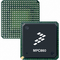
MPC885VR133 Freescale Semiconductor, MPC885VR133 Datasheet - Page 12

MPC885VR133
Manufacturer Part Number
MPC885VR133
Description
IC MPU POWERQUICC 133MHZ 357PBGA
Manufacturer
Freescale Semiconductor
Series
PowerQUICC Ir
Datasheet
1.MPC880VR80.pdf
(87 pages)
Specifications of MPC885VR133
Processor Type
MPC8xx PowerQUICC 32-Bit
Speed
133MHz
Voltage
3.3V
Mounting Type
Surface Mount
Package / Case
357-PBGA
Processor Series
MPC8xx
Core
MPC8xx
Data Bus Width
32 bit
Maximum Clock Frequency
133 MHz
Operating Supply Voltage
0 V to 5 V
Maximum Operating Temperature
+ 95 C
Mounting Style
SMD/SMT
Data Ram Size
8 KB
I/o Voltage
5 V
Interface Type
I2C, SPI, UART
Minimum Operating Temperature
0 C
Program Memory Size
8 KB
Program Memory Type
EPROM/Flash
Core Size
32 Bit
Cpu Speed
133MHz
Embedded Interface Type
I2C, JTAG, SPI, UART
Digital Ic Case Style
BGA
No. Of Pins
357
Rohs Compliant
Yes
For Use With
CWH-PPC-885XN-VX - BOARD EVAL QUICCSTART MPC885CWH-PPC-885XN-VE - BOARD EVAL QUICCSTART MPC885
Lead Free Status / RoHS Status
Lead free / RoHS Compliant
Features
-
Lead Free Status / Rohs Status
Lead free / RoHS Compliant
Available stocks
Company
Part Number
Manufacturer
Quantity
Price
Company:
Part Number:
MPC885VR133
Manufacturer:
Freescale Semiconductor
Quantity:
135
Company:
Part Number:
MPC885VR133
Manufacturer:
MOTOLOLA
Quantity:
853
Company:
Part Number:
MPC885VR133
Manufacturer:
Freescale Semiconductor
Quantity:
10 000
Part Number:
MPC885VR133
Manufacturer:
FREESCALE
Quantity:
20 000
Thermal Calculation and Measurement
1
2
3
4
5
6
7
For the following discussions, P
drivers.
7.1
An estimation of the chip junction temperature, T
where:
The junction-to-ambient thermal resistance is an industry standard value that provides a quick and easy
estimation of thermal performance. However, the answer is only an estimate; test cases have demonstrated
that errors of a factor of two (in the quantity T
12
Output high voltage, I
Output low voltage
I
I
I
I
I
OL
OL
OL
OL
OL
The difference between V
The signals PA[0:15], PB[14:31], PC[4:15], PD[3:15], PE(14:31), TDI, TDO, TCK, TRST, TMS, MII1_TXEN, MII_MDIO are 5-V
tolerant. The minimum voltage is still 2.0 V.
V
Input capacitance is periodically sampled.
A(0:31), TSIZ0/REG, TSIZ1, D(0:31), IRQ(2:4), IRQ6, RD/WR, BURST, IP_B(3:7), PA(0:11), PA13, PA15, PB(14:31),
PC(4:15), PD(3:15), PE(14:31), MII1_CRS, MII_MDIO, MII1_TXEN, and MII1_COL.
BDIP/GPL_B(5), BR, BG, FRZ/IRQ6, CS(0:7), WE(0:3), BS_A(0:3), GPL_A0/GPL_B0, OE/GPL_A1/GPL_B1,
GPL_A(2:3)/GPL_B(2:3)/CS(2:3), UPWAITA/GPL_A4, UPWAITB/GPL_B4, GPL_A5, ALE_A, CE1_A, CE2_A, OP(0:3), and
BADDR(28:30).
IL
= 2.0 mA (CLKOUT)
= 3.2 mA
= 5.3 mA
= 7.0 mA (TXD1/PA14, TXD2/PA12)
= 8.9 mA (TS, TA, TEA, BI, BB, HRESET, SRESET)
(max) for the I
Thermal Calculation and Measurement
T
R
P
A
D
θJA
Estimation with Junction-to-Ambient Thermal Resistance
= ambient temperature (ºC)
= power dissipation in package
5
6
= package junction-to-ambient thermal resistance (ºC/W)
T
J
2
C interface is 0.8 V rather than the 1.5 V as specified in the I
= T
OH
A
= –2.0 mA, except XTAL and open-drain pins
+ (R
DDL
Characteristic
MPC885/MPC880 PowerQUICC Hardware Specifications, Rev. 7
and V
θJA
Table 6. DC Electrical Specifications (continued)
The V
× P
DDSYN
D
= (V
D
)
DDSYN
cannot be more than 100 mV.
DDL
×
power dissipation is negligible.
I
DDL
J
– T
J
) + PI/O, where PI/O is the power dissipation of the I/O
NOTE
, in °C can be obtained from the following equation:
A
) are possible.
Symbol
2
V
V
C standard.
OH
OL
Min
2.4
—
Freescale Semiconductor
Max
0.5
—
Unit
V
V


