MPC8347VRADDB Freescale Semiconductor, MPC8347VRADDB Datasheet - Page 46
MPC8347VRADDB
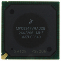
Manufacturer Part Number
MPC8347VRADDB
Description
IC MPU POWERQUICC II 620-PBGA
Manufacturer
Freescale Semiconductor
Series
PowerQUICC II PROr
Specifications of MPC8347VRADDB
Processor Type
MPC83xx PowerQUICC II Pro 32-Bit
Speed
266MHz
Voltage
1.2V
Mounting Type
Surface Mount
Package / Case
620-PBGA
Processor Series
MPC8xxx
Core
e300
Data Bus Width
32 bit
Development Tools By Supplier
MPC8349E-MITXE
Maximum Clock Frequency
266 MHz
Maximum Operating Temperature
+ 105 C
Mounting Style
SMD/SMT
I/o Voltage
1.8 V, 2.5 V, 3.3 V
Minimum Operating Temperature
0 C
Core Size
32 Bit
Program Memory Size
64KB
Cpu Speed
266MHz
Embedded Interface Type
I2C, SPI, USB, UART
Digital Ic Case Style
BGA
No. Of Pins
672
Rohs Compliant
Yes
Lead Free Status / RoHS Status
Lead free / RoHS Compliant
Features
-
Lead Free Status / Rohs Status
Lead free / RoHS Compliant
Available stocks
Company
Part Number
Manufacturer
Quantity
Price
Company:

Part Number:
MPC8347VRADDB
Manufacturer:
Freescale Semiconductor
Quantity:
135
Company:
Part Number:
MPC8347VRADDB
Manufacturer:
Freescale Semiconductor
Quantity:
10 000


I
Figure 31
Figure 32
46
2
Fall time of both SDA and SCL signals
Setup time for STOP condition
Bus free time between a STOP and START condition
Noise margin at the LOW level for each connected device (including
hysteresis)
Noise margin at the HIGH level for each connected device (including
hysteresis)
Notes:
1. The symbols for timing specifications follow the pattern of t
2. MPC8347E provides a hold time of at least 300 ns for the SDA signal (referred to the V
3. The maximum t
4. C
5.)The MPC8347E does not follow the “I
C
and t
respect to the time data input signals (D) reach the valid state (V) relative to the t
state or setup time. Also, t
goes invalid (X) relative to the t
timing (I2) for the time that the data with respect to the stop condition (P) reaches the valid state (V) relative to the t
reference (K) going to the high (H) state or setup time. For rise and fall times, the latter convention is used with the appropriate
letter: R (rise) or F (fall).
the undefined region of the falling edge of SCL.
B
SDA
SCL
= capacitance of one bus line in pF.
(first two letters of functional block)(reference)(state)(signal)(state)
provides the AC test load for the I
shows the AC timing diagram for the I
MPC8347E PowerQUICC™ II Pro Integrated Host Processor Hardware Specifications, Rev. 11
S
I2DVKH
t
I2CF
t
I2CL
t
I2SXKL
must be met only if the device does not stretch the LOW period (t
Output
I2SXKL
Parameter
Table 39. I
I2C
symbolizes I
clock reference (K) going to the low (L) state or hold time. Also, t
5
Figure 32. I
2
C-BUS Specifications” version 2.1 regarding the t
t
I2DXKL
2
C AC Electrical Specifications (continued)
Figure 31. I
2
t
Z
C timing (I2) for the time that the data with respect to the start condition (S)
I2DVKH
0
= 50 Ω
t
2
I2CH
2
C.
C Bus AC Timing Diagram
2
t
I2SXKL
2
C bus.
C AC Test Load
(first two letters of functional block)(signal)(state)(reference)(state)
for outputs. For example, t
Sr
t
I2SVKH
Symbol
R
t
t
t
I2KHKL
I2KHDX
I2PVKH
t
V
L
V
I2CF
NH
NL
= 50 Ω
I2C
1
clock reference (K) going to the high (H)
I2DVKH
0.1 × OV
0.2 × OV
t
IH
I2PVKH
OV
I2CL
I2CF
(min) of the SCL signal) to bridge
Min
0.6
1.3
DD
__
) of the SCL signal.
symbolizes I
t
AC parameter.
I2CR
/2
DD
DD
Freescale Semiconductor
I2PVKH
P
Max
2
t
300
I2CF
—
—
—
—
C timing (I2) with
symbolizes I
S
for inputs
I2C
Unit
ns
μs
μs
clock
V
V
2
C
Related parts for MPC8347VRADDB
Image
Part Number
Description
Manufacturer
Datasheet
Request
R

Part Number:
Description:
Integrated Host Processor Hardware Specifications
Manufacturer:
FREESCALE [Freescale Semiconductor, Inc]
Datasheet:

Part Number:
Description:
Manufacturer:
Freescale Semiconductor, Inc
Datasheet:
Part Number:
Description:
Manufacturer:
Freescale Semiconductor, Inc
Datasheet:
Part Number:
Description:
Manufacturer:
Freescale Semiconductor, Inc
Datasheet:
Part Number:
Description:
Manufacturer:
Freescale Semiconductor, Inc
Datasheet:
Part Number:
Description:
Manufacturer:
Freescale Semiconductor, Inc
Datasheet:
Part Number:
Description:
Manufacturer:
Freescale Semiconductor, Inc
Datasheet:
Part Number:
Description:
Manufacturer:
Freescale Semiconductor, Inc
Datasheet:
Part Number:
Description:
Manufacturer:
Freescale Semiconductor, Inc
Datasheet:
Part Number:
Description:
Manufacturer:
Freescale Semiconductor, Inc
Datasheet:
Part Number:
Description:
Manufacturer:
Freescale Semiconductor, Inc
Datasheet:
Part Number:
Description:
Manufacturer:
Freescale Semiconductor, Inc
Datasheet:
Part Number:
Description:
Manufacturer:
Freescale Semiconductor, Inc
Datasheet:
Part Number:
Description:
Manufacturer:
Freescale Semiconductor, Inc
Datasheet:
Part Number:
Description:
Manufacturer:
Freescale Semiconductor, Inc
Datasheet: