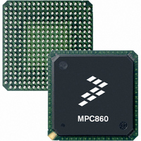
MPC866TCVR100A Freescale Semiconductor, MPC866TCVR100A Datasheet - Page 76

MPC866TCVR100A
Manufacturer Part Number
MPC866TCVR100A
Description
IC MPU POWERQUICC 100MHZ 357PBGA
Manufacturer
Freescale Semiconductor
Datasheet
1.MPC859DSLCVR50A.pdf
(96 pages)
Specifications of MPC866TCVR100A
Processor Type
MPC8xx PowerQUICC 32-Bit
Speed
100MHz
Voltage
1.8V
Mounting Type
Surface Mount
Package / Case
357-PBGA
Processor Series
MPC8xx
Core
MPC8xx
Data Bus Width
32 bit
Maximum Clock Frequency
100 MHz
Maximum Operating Temperature
+ 100 C
Mounting Style
SMD/SMT
Minimum Operating Temperature
- 40 C
Lead Free Status / RoHS Status
Lead free / RoHS Compliant
Features
-
Lead Free Status / Rohs Status
Lead free / RoHS Compliant
Available stocks
Company
Part Number
Manufacturer
Quantity
Price
Company:
Part Number:
MPC866TCVR100A
Manufacturer:
FREESCALE
Quantity:
201
Company:
Part Number:
MPC866TCVR100A
Manufacturer:
Freescale Semiconductor
Quantity:
135
Company:
Part Number:
MPC866TCVR100A
Manufacturer:
FREESCAL
Quantity:
364
Company:
Part Number:
MPC866TCVR100A
Manufacturer:
Freescale Semiconductor
Quantity:
10 000
FEC Electrical Characteristics
Figure 75
14.3 MII Async Inputs Signal Timing (MII_CRS, MII_COL)
Table 35
Figure 76
14.4 MII Serial Management Channel Timing (MII_MDIO, MII_MDC)
Table 36
maximum MDC frequency in excess of 2.5 MHz. The exact upper bound is under investigation.
76
Num
M10
M11
M12
MII_TXD[3:0] (outputs)
MII_TX_EN
MII_TX_ER
Num
MII_TX_CLK (input)
M9
shows the timing for on the MII async inputs signal.
shows the timing for the MII serial management channel signal. The FEC functions correctly with a
shows the MII transmit signal timing diagram.
shows the MII asynchronous inputs signal timing diagram.
MII_CRS, MII_COL
MII_MDC falling edge to MII_MDIO output invalid (minimum
propagation delay)
MII_MDC falling edge to MII_MDIO output valid (maximum
propagation delay)
MII_MDIO (input) to MII_MDC rising edge setup
MII_CRS, MII_COL minimum pulse width
Table 36. MII Serial Management Channel Timing
Figure 75. MII Transmit Signal Timing Diagram
MPC866/MPC859 Hardware Specifications, Rev. 2
Figure 76. MII Async Inputs Timing Diagram
Table 35. MII Async Inputs Signal Timing
Characteristic
Characteristic
M5
M6
M7
M9
M8
Min
1.5
Min
10
—
0
Max
—
Max
25
—
—
MII_TX_CLK period
Freescale Semiconductor
Unit
Unit
ns
ns
ns


