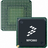
MPC860TCZQ50D4 Freescale Semiconductor, MPC860TCZQ50D4 Datasheet - Page 50

MPC860TCZQ50D4
Manufacturer Part Number
MPC860TCZQ50D4
Description
IC MPU POWERQUICC 50MHZ 357PBGA
Manufacturer
Freescale Semiconductor
Series
PowerQUICC Ir
Datasheet
1.MC860DECVR50D4R2.pdf
(80 pages)
Specifications of MPC860TCZQ50D4
Processor Type
MPC8xx PowerQUICC 32-Bit
Speed
50MHz
Voltage
3.3V
Mounting Type
Surface Mount
Package / Case
357-PBGA
Processor Series
MPC8xx
Core
MPC8xx
Data Bus Width
32 bit
Maximum Clock Frequency
50 MHz
Operating Supply Voltage
2.5 V, 3.3 V
Maximum Operating Temperature
+ 95 C
Mounting Style
SMD/SMT
Minimum Operating Temperature
- 40 C
Core Size
32 Bit
Program Memory Size
8KB
Cpu Speed
50MHz
Embedded Interface Type
Ethernet, I2C, SPI, UART
Digital Ic Case Style
BGA
No. Of Pins
357
Rohs Compliant
No
Family Name
MPC8xx
Device Core
PowerQUICC
Device Core Size
32b
Frequency (max)
50MHz
Instruction Set Architecture
RISC
Supply Voltage 1 (typ)
2.5/3.3V
Operating Supply Voltage (max)
3.465/3.6V
Operating Supply Voltage (min)
2/3.135V
Operating Temp Range
-40C to 95C
Operating Temperature Classification
Industrial
Mounting
Surface Mount
Pin Count
357
Package Type
BGA
Lead Free Status / RoHS Status
Contains lead / RoHS non-compliant
Features
-
Lead Free Status / Rohs Status
Lead free / RoHS Compliant
Available stocks
Company
Part Number
Manufacturer
Quantity
Price
Company:
Part Number:
MPC860TCZQ50D4
Manufacturer:
Freescale Semiconductor
Quantity:
10 000
CPM Electrical Characteristics
1
2
3
4
50
Num
The ratio SYNCCLK/L1RCLK must be greater than 2.5/1.
These specs are valid for IDL mode only.
Where P = 1/CLKOUT. Thus, for a 25-MHz CLKO1 rate, P = 40 ns.
These strobes and TxD on the first bit of the frame become valid after L1CLK edge or L1SYNC, whichever comes later.
84
85
86
87
88
(FE = 0, CE = 0)
(FE = 1, CE = 1)
L1CLK edge to L1CLKO valid (DSC = 1)
L1RQ valid before falling edge of L1TSYNC
L1GR setup time
L1GR hold time
L1CLK edge to L1SYNC valid (FSD = 00) CNT = 0000, BYT = 0, DSC = 0)
L1ST(4–1)
L1RSYNC
L1RCLK
L1RCLK
(Output)
L1RXD
(Input)
(Input)
(Input)
(Input)
Figure 51. SI Receive Timing Diagram with Normal Clocking (DSC = 0)
2
73
MPC860 PowerQUICC™ Family Hardware Specifications, Rev. 8
71
Characteristic
76
Table 19. SI Timing (continued)
75
74
72
4
70
BIT0
RFSD=1
78
77
71a
42.00
42.00
1.00
Min
—
—
All Frequencies
79
Freescale Semiconductor
30.00
Max
0.00
—
—
—
L1TCL
Unit
ns
ns
ns
ns
K


