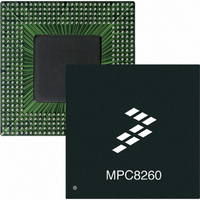
MPC8260AZUMHBB Freescale Semiconductor, MPC8260AZUMHBB Datasheet - Page 12

MPC8260AZUMHBB
Manufacturer Part Number
MPC8260AZUMHBB
Description
IC MPU POWERQUICC II 480-TBGA
Manufacturer
Freescale Semiconductor
Specifications of MPC8260AZUMHBB
Processor Type
MPC82xx PowerQUICC II 32-bit
Speed
266MHz
Voltage
2V
Mounting Type
Surface Mount
Package / Case
480-TBGA
Processor Series
MPC8xxx
Core
603e
Data Bus Width
32 bit
Maximum Clock Frequency
266 MHz
Maximum Operating Temperature
+ 105 C
Mounting Style
SMD/SMT
Minimum Operating Temperature
0 C
Leaded Process Compatible
Yes
Peak Reflow Compatible (260 C)
No
Rohs Compliant
No
For Use With
MPC8260ADS-TCOM - BOARD DEV ADS POWERQUICC II
Lead Free Status / RoHS Status
Contains lead / RoHS non-compliant
Features
-
Lead Free Status / Rohs Status
Lead free / RoHS Compliant
Available stocks
Company
Part Number
Manufacturer
Quantity
Price
Company:
Part Number:
MPC8260AZUMHBB
Manufacturer:
MOTOROLA
Quantity:
490
Company:
Part Number:
MPC8260AZUMHBB
Manufacturer:
Freescale Semiconductor
Quantity:
10 000
Part Number:
MPC8260AZUMHBB
Manufacturer:
FREE
Quantity:
20 000
1
Electrical and Thermal Characteristics
2.4
The following sections include illustrations and tables of clock diagrams, signals, and CPM outputs and
inputs for the 66 MHz MPC8260 device. Note that AC timings are based on a 50-pf load. Typical output
buffer impedances are shown in
Table 7
Table 8
12
Note:
sp36a
sp36b
sp38a
sp38b
Output specifications are measured from the 50% level of the rising edge of CLKIN to the 50% level of the signal. Timings are
measured at the pin.
sp40
sp42
Max
Spec Number
lists CPM output characteristics.
lists CPM input characteristics.
MPC8260 PowerQUICC II Integrated Communications Processor Hardware Specifications, Rev. 2
AC Electrical Characteristics
sp37a
sp37b
sp39a
sp39b
sp41
sp43
Min
It is recommended that the rise/fall time on CPM input pins should not
exceed 5 ns. This should be enforced especially on clock signals. Rise time
refers to signal transitions from 10% to 90% of VCC; fall time refers to
transitions from 90% to 10% of VCC.
FCC outputs—internal clock (NMSI)
FCC outputs—external clock (NMSI)
TDM outputs/SI
SCC/SMC/SPI/I2C outputs—internal clock (NMSI)
Ex_SCC/SMC/SPI/I2C outputs—external clock (NMSI)
PIO/TIMER/IDMA outputs
Table 7. AC Characteristics for CPM Outputs
1
60x bus
Local bus
Memory controller
Parallel I/O
Note:
Table
NOTE: Rise/Fall Time on CPM Input Pins
These are typical values at 65° C. The impedance
may vary by ±25% with process and temperature.
Table 6. Output Buffer Impedances
Output Buffers
6.
Characteristic
Typical Impedance (Ω)
40
40
40
46
1
1
Max Delay (ns)
66 MHz
14
25
19
19
14
6
Freescale Semiconductor
Min Delay (ns)
66 MHz
1
2
5
1
2
1


