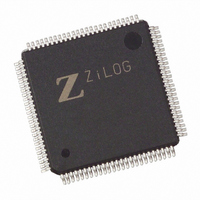
Z8018233ASC00TR Zilog, Z8018233ASC00TR Datasheet - Page 9

Z8018233ASC00TR
Manufacturer Part Number
Z8018233ASC00TR
Description
IC Z180 MPU 100LQFP
Manufacturer
Zilog
Datasheet
1.Z8018233FSG.pdf
(109 pages)
Specifications of Z8018233ASC00TR
Processor Type
Z180
Features
Smart Peripheral Controller
Speed
33MHz
Voltage
5V
Mounting Type
Surface Mount
Package / Case
100-LQFP
Lead Free Status / RoHS Status
Contains lead / RoHS non-compliant
Available stocks
Company
Part Number
Manufacturer
Quantity
Price
PARALLEL PORTS
/W//REQB. Wait/Request (output, open drain when
programmed for the Wait function, driven High or Low
when programmed for a Request function). This pin is
similar in functionality to /W//REQA but is applicable on
16550 MIMIC INTERFACE SIGNALS
HD7-HD0. Host Data Bus (input/output, tri-state). In Z80182/
Z8L182 mode 1, the host data bus is used to communicate
between the 16550 MIMIC interface and the PC/XT/AT. It
is multiplexed with the PA7-PA0 of parallel Port A when the
Z80182/Z8L182 is in mode 0.
/HDDIS. Host Driver Disable (output, active Low). In Z80182/
Z8L182 mode 1, this signal goes Low whenever the
PC/XT/AT is reading data from the 16550 MIMIC interface.
In Z80182/Z8L182 mode 0, this pin is multiplexed with the
ESCC
HA2-HA0. Host Address (input). In Z80182/Z8L182 mode
1, these pins are the address inputs to the 16550 MIMIC
interface. This address determines which register the
PC/XT/AT accesses. HA0 is multiplexed with /TRxCB on
the /TRxCB/HA0 pin; HA1 is multiplexed with RxDB on the
RxDB/HA1 pin; HA2 is multiplexed with /RTxCB on the
/RTxCB/HA2 pin.
/HCS. Host Chip Select (input, active Low). In Z80182/
Z8L182 mode 1, this input is used by the PC/XT/AT to
select the 16550 MIMIC interface for an access. In Z80182/
Z8L182 mode 0, it is multiplexed with the ESCC /SYNCB
signal on the SYNCB//HCS pin.
/HWR. Host Write (Input, active Low). In Z80182/Z8L182
mode 1, this input is used by the PC/XT/AT to signal the
16550 MIMIC interface that a write operation is taking
place. In Z80182/Z8L182 mode 0, this input is multiplexed
with the ESCC /CTSB signal on the /CTSB//HWR pin.
PA7-PA0. Parallel Port A (input/output). These lines can be
configured as inputs or outputs on a bit-by-bit basis when
the Z80182/Z8L182 is operated in mode 0. These pins are
multiplexed with the HD7-HD0 when the Z80182/Z8L182 is
in mode 1.
PB7-PB0. Parallel Port B (input/output). These lines can be
configured as inputs or outputs on a bit-by-bit basis when
the Port function is selected in the System Configuration
register. The pins are multiplexed with the following Z180
peripheral functions: /RTS0, /CTS0, /DCD0, TxA0, RxA0,
TxA1, RxA1, (RxS//CTS1).
DS971820600
Zilog
™
TxDB signal on the TxDB//HDDIS pin.
PS009801-0301
P R E L I M I N A R Y
channel B. The /W//REQB signal is multiplexed with the
Z180 MPU CKS signal and the 16550 MIMIC interface
/HTxRDY signal on the CKS//W//REQB//HTxRDY pin.
/HRD. Host Read (input, active Low). In Z80182/Z8L182
mode 1, this input is used by the PC/XT/AT to signal the
16550 MIMIC interface that a read operation is taking
place. In Z80182/Z8L182 mode 0, this pin is multiplexed
with the ESCC /DCDB signal on the /DCDB//HRD pin.
HINTR. Host Interrupt (output, active High). In Z80182/
Z8L182 mode 1, this output is used by the 16550 MIMIC
interface to signal the PC/XT/AT that an interrupt is pending.
In Z80182/Z8L182 mode 0, this pin is multiplexed with the
ESCC (/DTR//REQB) signal and the Z180 MPU TxS signal
on the TxS//DTR//REQB//HINTR pin.
/HTxRDY. Host Transmit Ready (output, active Low). In
Z80182/Z8L182 mode 1, this output is used by the 16550
MIMIC in DMA mode to signal the PC/XT/AT that the
Transmit Holding Register is empty. In Z80182/Z8L182
mode 0, this pin is multiplexed with the ESCC (/W//REQB)
signal and the Z180 MPU CKS signal on the CKS//W//
REQB//HTxRDY pin.
/HRxRDY. Host Receive Ready (output, active Low). In
Z80182/Z8L182 mode 1, this output is used by the 16550
MIMIC interface in DMA mode to signal the PC/XT/AT that
a data byte is ready in the Receive Buffer. In Z80182/
Z8L182 mode 0, this pin is multiplexed with the ESCC
/RTSB signal and the Z180 MPU /TEND1 signal on the
/TEND1/RTSB /HRxRDY pin.
PC7-PC0. Parallel Port C (input/output). These lines can
be configured as inputs or outputs on a bit-by-bit basis for
bits PC5-PC0. Bits PC7 and PC6 are input only and read
the level of the external /INT2 and /INT1 pins. When /INT2
and/or /INT1 are in edge capture mode, writing a 1 to the
respective PC7, PC6 bit clears the interrupt capture latch;
writing a 0 has no effect. Bits PC5-PC0 are multiplexed with
the following pins from ESCC channel A: (/W//REQA),
/SYNCA, (/DTR//REQA), /RTSA, /MWR, /CTSA, /DCDA.
The Port function is selected through a bit in the System
Configuration Register.
Z
ILOG
I
NTELLIGENT
Z80182/Z8L182
P
ERIPHERAL
3-9


