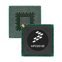
MPC8313CVRADDB Freescale Semiconductor, MPC8313CVRADDB Datasheet - Page 78

MPC8313CVRADDB
Manufacturer Part Number
MPC8313CVRADDB
Description
MPU POWERQUICC II PRO 516-PBGA
Manufacturer
Freescale Semiconductor
Datasheet
1.MPC8313CZQAFFB.pdf
(100 pages)
Specifications of MPC8313CVRADDB
Processor Type
MPC83xx PowerQUICC II Pro 32-Bit
Speed
267MHz
Voltage
0.95 V ~ 1.05 V
Mounting Type
Surface Mount
Package / Case
516-PBGA
Processor Series
MPC8xxx
Core
e300
Data Bus Width
32 bit
Development Tools By Supplier
MPC8313E-RDB
Maximum Clock Frequency
400 MHz
Operating Supply Voltage
- 0.3 V to + 1.26 V
Maximum Operating Temperature
+ 105 C
Mounting Style
SMD/SMT
Data Ram Size
16 KB
I/o Voltage
2.5 V
Interface Type
I2C, SPI, UART
Minimum Operating Temperature
- 40 C
Program Memory Type
EEPROM/Flash
Lead Free Status / RoHS Status
Lead free / RoHS Compliant
Features
-
Lead Free Status / Rohs Status
Lead free / RoHS Compliant
Available stocks
Company
Part Number
Manufacturer
Quantity
Price
Company:
Part Number:
MPC8313CVRADDB
Manufacturer:
FREESCAL
Quantity:
672
Company:
Part Number:
MPC8313CVRADDB
Manufacturer:
Freescale Semiconductor
Quantity:
10 000
Clocking
The primary clock source for the MPC8313E can be one of two inputs, SYS_CLK_IN or PCI_CLK,
depending on whether the device is configured in PCI host or PCI agent mode. When the device is
configured as a PCI host device, SYS_CLK_IN is its primary input clock. SYS_CLK_IN feeds the PCI
clock divider (÷2) and the multiplexors for PCI_SYNC_OUT and PCI_CLK_OUT. The
CFG_CLKIN_DIV configuration input selects whether SYS_CLK_IN or SYS_CLK_IN/2 is driven out
on the PCI_SYNC_OUT signal. The OCCR[PCICOEn] parameters select whether the PCI_SYNC_OUT
is driven out on the PCI_CLK_OUTn signals.
PCI_SYNC_OUT is connected externally to PCI_SYNC_IN to allow the internal clock subsystem to
synchronize to the system PCI clocks. PCI_SYNC_OUT must be connected properly to PCI_SYNC_IN,
with equal delay to all PCI agent devices in the system, to allow the device to function. When the device
is configured as a PCI agent device, PCI_CLK is the primary input clock. When the device is configured
as a PCI agent device the SYS_CLK_IN signal should be tied to VSS.
As shown in
loop (PLL) and the clock unit to create the coherent system bus clock (csb_clk), the internal clock for the
DDR controller (ddr_clk), and the internal clock for the local bus interface unit (lbc_clk).
The csb_clk frequency is derived from a complex set of factors that can be simplified into the following
equation:
In PCI host mode, PCI_SYNC_IN × (1 + ~CFG_CLKIN_DIV) is the SYS_CLK_IN frequency.
The csb_clk serves as the clock input to the e300 core. A second PLL inside the e300 core multiplies up
the csb_clk frequency to create the internal clock for the e300 core (core_clk). The system and core PLL
multipliers are selected by the SPMF and COREPLL fields in the reset configuration word low (RCWL)
which is loaded at power-on reset or by one of the hard-coded reset options. See Chapter 4, “Reset,
Clocking, and Initialization,” in the MPC8313E PowerQUICC II Pro Integrated Processor Family
Reference Manual, for more information on the clock subsystem.
The internal ddr_clk frequency is determined by the following equation:
Note that ddr_clk is not the external memory bus frequency; ddr_clk passes through the DDR clock divider
(÷2) to create the differential DDR memory bus clock outputs (MCK and MCK). However, the data rate
is the same frequency as ddr_clk.
The internal lbc_clk frequency is determined by the following equation:
Note that lbc_clk is not the external local bus frequency; lbc_clk passes through the a LBC clock divider
to create the external local bus clock outputs (LCLK[0:1]). The LBC clock divider ratio is controlled by
LCCR[CLKDIV].
In addition, some of the internal units may be required to be shut off or operate at lower frequency than
the csb_clk frequency. Those units have a default clock ratio that can be configured by a memory mapped
register after the device comes out of reset.
frequency.
78
csb_clk = {PCI_SYNC_IN × (1 + ~CFG_CLKIN_DIV)} × SPMF
ddr_clk = csb_clk × (1 + RCWL[DDRCM])
lbc_clk = csb_clk × (1 + RCWL[LBCM])
Figure
MPC8313E PowerQUICC
57, the primary clock input (frequency) is multiplied up by the system phase-locked
™
II Pro Processor Hardware Specifications, Rev. 3
Table 64
specifies which units have a configurable clock
Freescale Semiconductor


