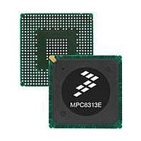
MPC8313CVRADDB Freescale Semiconductor, MPC8313CVRADDB Datasheet - Page 95

MPC8313CVRADDB
Manufacturer Part Number
MPC8313CVRADDB
Description
MPU POWERQUICC II PRO 516-PBGA
Manufacturer
Freescale Semiconductor
Datasheet
1.MPC8313CZQAFFB.pdf
(100 pages)
Specifications of MPC8313CVRADDB
Processor Type
MPC83xx PowerQUICC II Pro 32-Bit
Speed
267MHz
Voltage
0.95 V ~ 1.05 V
Mounting Type
Surface Mount
Package / Case
516-PBGA
Processor Series
MPC8xxx
Core
e300
Data Bus Width
32 bit
Development Tools By Supplier
MPC8313E-RDB
Maximum Clock Frequency
400 MHz
Operating Supply Voltage
- 0.3 V to + 1.26 V
Maximum Operating Temperature
+ 105 C
Mounting Style
SMD/SMT
Data Ram Size
16 KB
I/o Voltage
2.5 V
Interface Type
I2C, SPI, UART
Minimum Operating Temperature
- 40 C
Program Memory Type
EEPROM/Flash
Lead Free Status / RoHS Status
Lead free / RoHS Compliant
Features
-
Lead Free Status / Rohs Status
Lead free / RoHS Compliant
Available stocks
Company
Part Number
Manufacturer
Quantity
Price
Company:
Part Number:
MPC8313CVRADDB
Manufacturer:
FREESCAL
Quantity:
672
Company:
Part Number:
MPC8313CVRADDB
Manufacturer:
Freescale Semiconductor
Quantity:
10 000
Freescale Semiconductor
Number
Rev.
1
3/2008
Date
MPC8313E PowerQUICC
• Replaced OVDD with NV
• Added XCOREVDD and XPADVDD to Table 1
• Moved VDD and VDDC to the top of the table before SerDes supplies in Table 2
• In Table 2 split DDR row into two from total current requirement of 425 mA. One for DDR1 (131 mA)
• In Table 2 corrected current requirement numbers for NV
• In Table 2 corrected Vdd and Vddc current requirements from 560 mA and 454 mA to 469 and
• In Table 2, added row stating junction temperature range of 0 to 105•C. Added footnote 2 stating
• In Section 2.1.2, “Power Supply Voltage Specification,” added a note describing the purpose of
• In Section 3, “Power Characteristics,” added a note describing the purpose of Table 5.
• Rewrote Section 2.2, “Power Sequencing,” and added Figure 3.
• In Table 4, added “but do include core, USB PLL, and a portion of SerDes digital power...” to Note 1.
• In Table 4 corrected “Typical power” to “Maximum power” in note 2 and added a note for Typical
• In Table 4 removed 266-MHz row as 266-MHz core parts are not offered.
• In Table 5, moved Local bus typical power dissipation under LVdd.
• Added Table 6 to show the low power mode power dissipation for D3warm mode.
• In Table 8 corrected SYS_CLK_IN frequency range from 25–66 MHz to 24–66.67 MHz.
• Added Section 8.4, “eTSEC IEEE 1588 AC Specifications”
• In Table 42 changed minimum value of USB input hold t
• Added Table 43 and Table 44 showing USB clock in specifications
• In Table 46, added rows for t
• In Table 50, removed row for rise time (t
• In Table 56, added a note stating: “This specification only applies to GPIO pins that are operating
• Added Table 57 to show DC characteristics for GPIO pins supplied by a 2.5-V supply. Same as
• In Section 20, “Clocking,” corrected the sentence “When the device is configured as a PCI agent
• Added “Value is decided by RCWLR[COREPLL]” to note 1 of Figure 57
• Added paragraph and Figure 59 to Section 22.2, “PLL Power Supply Filtering.”
• Added Section 22.4, “SerDes Block Power Supply Decoupling Recommendations
• Removed the two figures on PCI undershoot/overshoot voltages and maximum AC waveforms from
and other for DDR2 (140 mA).
to 16 mA, LV
377 mA, respectively. Corrected Avdd1 and Avdd2 current requirements from 10 mA to 2–3 mA, and
XCOREVDD from 100 mA to 170 mA.
GPIO pins may operate from 2.5-V supply as well when configured for different functionality.
Table 2.
Power.
Figure 40.
that the device does not follow the I2C-BUS Specifications version 2.1 regarding the t
parameter.
from a 3.3-V supply. See Table 63 for the power supply listed for the individual GPIO signal.” [
eTSEC DC characteristics when operating at 2.5 V.
device, PCI_SYNC_IN is the primary input clock.” to state “When the device is configured as a PCI
agent device, PCI_CLK is the primary input clock.”
Section 2.1.2, “Power Supply Voltage Specification,”
Table 73. Document Revision History (continued)
DDA
from 85 mA to 22 mA and LV
™
II Pro Processor Hardware Specifications, Rev. 3
DD
everywhere
LALEHOV
Substantive Change(s)
, t
LALETOT1,
I2CR
). Removed minimum value of t
DDB
t
LALETOT2,
from 85 mA to 44 mA.
USIXKH
DD
and t
from 27 mA to 74 mA, LV
from 0 to 1ns
LALETOT3
C. Added footnote 2 stating
parameters. Added
I2CF
Document Revision History
. Added note 5 stating
DD
I2CF
from 60 mA
AC
95


