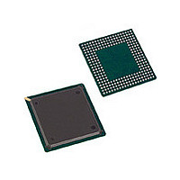
MPC850DSLZQ50BU Freescale Semiconductor, MPC850DSLZQ50BU Datasheet - Page 9

MPC850DSLZQ50BU
Manufacturer Part Number
MPC850DSLZQ50BU
Description
IC MPU PWRQUICC 50MHZ 256-PBGA
Manufacturer
Freescale Semiconductor
Specifications of MPC850DSLZQ50BU
Processor Type
MPC8xx PowerQUICC 32-Bit
Speed
50MHz
Voltage
3.3V
Mounting Type
Surface Mount
Package / Case
256-PBGA
Family Name
MPC8xx
Device Core
PowerQUICC
Device Core Size
32b
Frequency (max)
50MHz
Instruction Set Architecture
RISC
Supply Voltage 1 (typ)
3.3V
Operating Supply Voltage (max)
3.465V
Operating Supply Voltage (min)
3.135V
Operating Temp Range
0C to 95C
Operating Temperature Classification
Commercial
Mounting
Surface Mount
Pin Count
256
Package Type
BGA
Lead Free Status / RoHS Status
Contains lead / RoHS non-compliant
Features
-
Lead Free Status / Rohs Status
Not Compliant
Available stocks
Company
Part Number
Manufacturer
Quantity
Price
Company:
Part Number:
MPC850DSLZQ50BU
Manufacturer:
FREESCAL
Quantity:
364
Company:
Part Number:
MPC850DSLZQ50BU
Manufacturer:
Freescale Semiconductor
Quantity:
10 000
Part Number:
MPC850DSLZQ50BU
Manufacturer:
FREESCALE
Quantity:
20 000
5
The average chip-junction temperature
T
where
T
Freescale Semiconductor
A
J
= T
= Ambient temperature
1
2
3 The MPC850 IBIS model must be used to accurately model the behavior of the Clkout output driver for the full and
Input low voltage
EXTAL, EXTCLK input high voltage
Input leakage current, Vin = 5.5 V (Except TMS, TRST, DSCK
and DSDI pins)
Input leakage current, Vin = 3.6V (Except TMS, TRST, DSCK
and DSDI pins)
Input leakage current, Vin = 0V (Except TMS, TRST, DSCK
and DSDI pins)
Input capacitance
Output high voltage, IOH = -2.0 mA, VDDH = 3.0V
except XTAL, XFC, and open-drain pins
Output low voltage
CLKOUT
IOL = 3.2 mA
IOL = 5.3 mA
IOL = 7.0 mA PA[14]/USBOE, PA[12]/TXD2
IOL = 8.9 mA TS, TA, TEA, BI, BB, HRESET, SRESET
IP_B2/IOIS16_B/AT2, IP_B3/IWP2/VF2, IP_B4/LWP0/VF0, IP_B5/LWP1/VF1, IP_B6/DSDI/AT0, IP_B7/PTR/AT3,
PA[15]/USBRXD, PA[13]/RXD2, PA[9]/L1TXDA/SMRXD2, PA[8]/L1RXDA/SMTXD2,
PA[7]/CLK1/TIN1/L1RCLKA/BRGO1, PA[6]/CLK2/TOUT1/TIN3, PA[5]/CLK3/TIN2/L1TCLKA/BRGO2,
PA[4]/CLK4/TOUT2/TIN4, PB[31]/SPISEL, PB[30]/SPICLK/TXD3, PB[29]/SPIMOSI /RXD3,
PB[28]/SPIMISO/BRGO3, PB[27]/I2CSDA/BRGO1, PB[26]/I2CSCL/BRGO2, PB[25]/SMTXD1/TXD3,
PB[24]/SMRXD1/RXD3, PB[23]/SMSYN1/SDACK1, PB[22]/SMSYN2/SDACK2, PB[19]/L1ST1,
PB[18]/RTS2/L1ST2, PB[17]/L1ST3, PB[16]/L1RQa/L1ST4, PC[15]/DREQ0/L1ST5, PC[14]/DREQ1/RTS2/L1ST6,
PC[13]/L1ST7/RTS3, PC[12]/L1RQa/L1ST8, PC[11]/USBRXP, PC[10]/TGATE1/USBRXN, PC[9]/CTS2,
PC[8]/CD2/TGATE1, PC[7]/USBTXP, PC[6]/USBTXN, PC[5]/CTS3/L1TSYNCA/SDACK1, PC[4]/CD3/L1RSYNCA,
PD[15], PD[14], PD[13], PD[12], PD[11], PD[10], PD[9], PD[8], PD[7], PD[6], PD[5], PD[4], PD[3]
WE2/BS_AB2/PCOE, WE3/BS_AB3/PCWE, GPL_A0/GPL_B0, OE/GPL_A1/GPL_B1,
GPL_A[2:3]/GPL_B[2:3]/CS[2:3], UPWAITA/GPL_A4/AS, UPWAITB/GPL_B4, GPL_A5, ALE_B/DSCK/AT1,
OP2/MODCK1/STS, OP3/MODCK2/DSDO
half drive setting. Due to the nature of the Clkout output buffer, IOH and IOL for Clkout should be extracted from the
IBIS model at any output voltage level.
A[6:31], TSIZ0/REG, TSIZ1, D[0:31], DP[0:3]/IRQ[3:6], RD/WR, BURST, RSV/IRQ2, IP_B[0:1]/IWP[0:1]/VFLS[0:1],
BDIP/GPL_B5, BR, BG, FRZ/IRQ6, CS[0:5], CS6/CE1_B, CS7/CE2_B, WE0/BS_AB0/IORD, WE1/BS_AB1/IOWR,
A
Power Considerations
+ (P
MPC850 PowerQUICC™ Integrated Communications Processor Hardware Specifications, Rev. 2
3
D
•
1
2
θ
JA
)(1)
Characteristic
,
°C
Table 5. DC Electrical Specifications (continued)
,
T
J
,
in °C can be obtained from the equation:
Symbol
VIHC
VOH
VOL
VIL
C
I
I
I
In
In
in
in
0.7*(VCC)
GND
Min
2.4
—
—
—
—
—
VCC+0.3
Power Considerations
Max
100
0.8
0.5
10
10
20
—
Unit
µA
µA
µA
pF
V
V
V
V
9


