MPC8347CVRAGDB Freescale Semiconductor, MPC8347CVRAGDB Datasheet - Page 47
MPC8347CVRAGDB
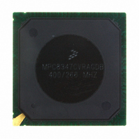
Manufacturer Part Number
MPC8347CVRAGDB
Description
IC MPU POWERQUICC II 620-PBGA
Manufacturer
Freescale Semiconductor
Series
PowerQUICC II PROr
Specifications of MPC8347CVRAGDB
Processor Type
MPC83xx PowerQUICC II Pro 32-Bit
Speed
400MHz
Voltage
1.2V
Mounting Type
Surface Mount
Package / Case
620-PBGA
Core Size
32 Bit
Program Memory Size
64KB
Cpu Speed
400MHz
Embedded Interface Type
I2C, SPI, USB, UART
Digital Ic Case Style
BGA
No. Of Pins
672
Rohs Compliant
Yes
Lead Free Status / RoHS Status
Lead free / RoHS Compliant
Features
-
Available stocks
Company
Part Number
Manufacturer
Quantity
Price
Company:

Part Number:
MPC8347CVRAGDB
Manufacturer:
FREESCA
Quantity:
13
Company:
Part Number:
MPC8347CVRAGDB
Manufacturer:
Freescale Semiconductor
Quantity:
10 000


13 PCI
This section describes the DC and AC electrical specifications for the PCI bus of the MPC8347E.
13.1
Table 40
13.2
This section describes the general AC timing parameters of the PCI bus of the MPC8347E. Note that the
PCI_CLK or PCI_SYNC_IN signal is used as the PCI input clock depending on whether the MPC8347E
is configured as a host or agent device.
Freescale Semiconductor
High-level input voltage
Low-level input voltage
Input current
High-level output voltage
Low-level output voltage
Note:
1. The symbol V
Clock to output valid
Output hold from clock
Clock to output high impedance
Input setup to clock
provides the DC electrical characteristics for the PCI interface of the MPC8347E.
PCI DC Electrical Characteristics
PCI AC Electrical Specifications
MPC8347E PowerQUICC™ II Pro Integrated Host Processor Hardware Specifications, Rev. 11
Parameter
IN
, in this case, represents the OV
Parameter
Table 41. PCI AC Timing Specifications at 66 MHz
Table 40. PCI DC Electrical Characteristics
Symbol
V
V
V
V
I
IN
OH
OL
IH
IL
Table 41
IN
symbol referenced in
V
IN
V
provides the PCI AC timing specifications at 66 MHz.
Symbol
t
V
1
t
OUT
t
PCKHOV
PCKHOX
t
= 0 V or V
PCKHOZ
Test Condition
PCIVKH
OUT
I
OH
I
OV
OV
OL
≥ V
= –100 μA
≤ V
DD
DD
= 100 μA
OH
2
OL
= min,
= min,
IN
(min) or
(max)
= OV
Table
DD
Min
3.0
—
—
1
1.
OV
DD
–0.3
Min
—
—
2
– 0.2
1
Max
6.0
14
—
—
OV
DD
Max
0.8
0.2
±5
—
Unit
+ 0.3
ns
ns
ns
ns
Notes
Unit
3, 4
3, 5
μA
V
V
V
V
3
3
PCI
47
Related parts for MPC8347CVRAGDB
Image
Part Number
Description
Manufacturer
Datasheet
Request
R

Part Number:
Description:
Manufacturer:
Freescale Semiconductor, Inc
Datasheet:
Part Number:
Description:
Manufacturer:
Freescale Semiconductor, Inc
Datasheet:
Part Number:
Description:
Manufacturer:
Freescale Semiconductor, Inc
Datasheet:
Part Number:
Description:
Manufacturer:
Freescale Semiconductor, Inc
Datasheet:
Part Number:
Description:
Manufacturer:
Freescale Semiconductor, Inc
Datasheet:
Part Number:
Description:
Manufacturer:
Freescale Semiconductor, Inc
Datasheet:
Part Number:
Description:
Manufacturer:
Freescale Semiconductor, Inc
Datasheet:
Part Number:
Description:
Manufacturer:
Freescale Semiconductor, Inc
Datasheet:
Part Number:
Description:
Manufacturer:
Freescale Semiconductor, Inc
Datasheet:
Part Number:
Description:
Manufacturer:
Freescale Semiconductor, Inc
Datasheet:
Part Number:
Description:
Manufacturer:
Freescale Semiconductor, Inc
Datasheet:
Part Number:
Description:
Manufacturer:
Freescale Semiconductor, Inc
Datasheet:
Part Number:
Description:
Manufacturer:
Freescale Semiconductor, Inc
Datasheet:
Part Number:
Description:
Manufacturer:
Freescale Semiconductor, Inc
Datasheet:
Part Number:
Description:
Manufacturer:
Freescale Semiconductor, Inc
Datasheet: