MPC8347CVRAGDB Freescale Semiconductor, MPC8347CVRAGDB Datasheet - Page 8
MPC8347CVRAGDB
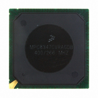
Manufacturer Part Number
MPC8347CVRAGDB
Description
IC MPU POWERQUICC II 620-PBGA
Manufacturer
Freescale Semiconductor
Series
PowerQUICC II PROr
Specifications of MPC8347CVRAGDB
Processor Type
MPC83xx PowerQUICC II Pro 32-Bit
Speed
400MHz
Voltage
1.2V
Mounting Type
Surface Mount
Package / Case
620-PBGA
Core Size
32 Bit
Program Memory Size
64KB
Cpu Speed
400MHz
Embedded Interface Type
I2C, SPI, USB, UART
Digital Ic Case Style
BGA
No. Of Pins
672
Rohs Compliant
Yes
Lead Free Status / RoHS Status
Lead free / RoHS Compliant
Features
-
Available stocks
Company
Part Number
Manufacturer
Quantity
Price
Company:

Part Number:
MPC8347CVRAGDB
Manufacturer:
FREESCA
Quantity:
13
Company:
Part Number:
MPC8347CVRAGDB
Manufacturer:
Freescale Semiconductor
Quantity:
10 000


Electrical Characteristics
2.1.2
Table 2
Table 2
conditions is not guaranteed.
Figure 2
8
Core supply voltage
PLL supply voltage
DDR DRAM I/O supply voltage
Three-speed Ethernet I/O supply voltage
Three-speed Ethernet I/O supply voltage
PCI, local bus, DUART, system control and power
management, I
Note:
1
GV
negative direction.
DD
, LV
provides the recommended operating conditions for the MPC8347E. Note that the values in
are the recommended and tested operating conditions. Proper device operation outside these
shows the undershoot and overshoot voltages at the interfaces of the MPC8347E.
DD
MPC8347E PowerQUICC™ II Pro Integrated Host Processor Hardware Specifications, Rev. 11
Power Supply Voltage Specification
, OV
2
C, and JTAG I/O voltage
DD
V
V
Note:
, AV
1. t
IH
IL
Characteristic
DD
interface
Figure 2. Overshoot/Undershoot Voltage for GV
G/L/OV
, and V
G/L/OV
GND – 0.3 V
GND – 0.7 V
refers to the clock period associated with the bus clock interface.
G/L/OV
DD
DD
Table 2. Recommended Operating Conditions
DD
+ 20%
must track each other and must vary in the same direction—either in the positive or
+ 5%
GND
DD
Not to Exceed 10%
Symbol
LV
LV
of t
GV
OV
AV
V
DD
DD1
DD2
DD
interface
DD
DD
1
Recommended
2.5 V ± 125 mV
3.3 V ± 330 mV
2.5 V ± 125 mV
3.3 V ± 330 mV
2.5 V ± 125 mV
3.3 V ± 330 mV
1.2 V ± 60 mV
1.2 V ± 60 mV
DD
/OV
Value
DD
/LV
DD
Freescale Semiconductor
Unit
V
V
V
V
V
V
Notes
1
1
Related parts for MPC8347CVRAGDB
Image
Part Number
Description
Manufacturer
Datasheet
Request
R

Part Number:
Description:
Manufacturer:
Freescale Semiconductor, Inc
Datasheet:
Part Number:
Description:
Manufacturer:
Freescale Semiconductor, Inc
Datasheet:
Part Number:
Description:
Manufacturer:
Freescale Semiconductor, Inc
Datasheet:
Part Number:
Description:
Manufacturer:
Freescale Semiconductor, Inc
Datasheet:
Part Number:
Description:
Manufacturer:
Freescale Semiconductor, Inc
Datasheet:
Part Number:
Description:
Manufacturer:
Freescale Semiconductor, Inc
Datasheet:
Part Number:
Description:
Manufacturer:
Freescale Semiconductor, Inc
Datasheet:
Part Number:
Description:
Manufacturer:
Freescale Semiconductor, Inc
Datasheet:
Part Number:
Description:
Manufacturer:
Freescale Semiconductor, Inc
Datasheet:
Part Number:
Description:
Manufacturer:
Freescale Semiconductor, Inc
Datasheet:
Part Number:
Description:
Manufacturer:
Freescale Semiconductor, Inc
Datasheet:
Part Number:
Description:
Manufacturer:
Freescale Semiconductor, Inc
Datasheet:
Part Number:
Description:
Manufacturer:
Freescale Semiconductor, Inc
Datasheet:
Part Number:
Description:
Manufacturer:
Freescale Semiconductor, Inc
Datasheet:
Part Number:
Description:
Manufacturer:
Freescale Semiconductor, Inc
Datasheet: