MPC8540PX667LC Freescale Semiconductor, MPC8540PX667LC Datasheet - Page 12
MPC8540PX667LC
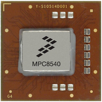
Manufacturer Part Number
MPC8540PX667LC
Description
IC MPU 32BIT 667MHZ 783-FCPBGA
Manufacturer
Freescale Semiconductor
Specifications of MPC8540PX667LC
Processor Type
MPC85xx PowerQUICC III 32-Bit
Speed
667MHz
Voltage
1.2V
Mounting Type
Surface Mount
Package / Case
783-FCPBGA
For Use With
MPC8548CDS - DEV TOOLS CDS FOR 8548MPC8540ADS-BGA - BOARD APPLICATION DEV 8540CWH-PPC-8540N-VE - KIT EVAL SYSTEM MPC8540
Lead Free Status / RoHS Status
Lead free / RoHS Compliant
Features
-
Available stocks
Company
Part Number
Manufacturer
Quantity
Price
Company:

Part Number:
MPC8540PX667LC
Manufacturer:
Freescale Semiconductor
Quantity:
10 000


MPC8540 Architecture Overview
The L2 status array maintains status bits for each line to determine the status of the line. Different combinations of
these bits result in different L2 states. Note that because the cache is always write-through, there is no modified state.
The status bits include the following:
All accesses to the L2 memory are fully pipelined so back-to-back loads and stores can have single-cycle throughput.
The cache can be configured to allocate instructions-only, data-only, or both. It can also be configured to allocate
global I/O writes that correspond to a programmable address window or that use a special transaction type (stashing).
In this way, DMA engines or I/O devices can force data into the cache.
Line locks can be set in a variety of ways. The Book E architecture defines instructions that explicitly set and clear
locks in the L2. These instructions are supported by the core complex and the L2 controller. In addition, the L2
controller can be configured to lock all lines that fall into either of two specified address ranges when the line is
allocated. Finally, the entire cache can be locked by writing to a configuration register in the L2 cache controller.
The status array tracks line locks as either instruction locks or data locks for each line, and the status array supports
flash clearing of all instruction locks or data locks separately by writes to configuration registers in the L2 controller.
3.3 e500 Coherency Module (ECM)
The e500 coherency module (ECM) provides a mechanism for I/O-initiated transactions to snoop the bus between
the e500 core and the integrated L2 cache in order to maintain coherency across local cacheable memory. It also
provides a flexible switch-type structure for core and I/O-initiated transactions to be routed or dispatched to target
modules on the device.
3.4 DDR SDRAM Controller
The MPC8540 supports DDR-I SDRAM that operates at up to 166 MHz (333-MHz data rate). The memory interface
controls main memory accesses and provides for a maximum of 3.5 Gbytes of main memory. The memory controller
can be configured to support the various memory sizes through software initialization of on-chip configuration
registers.
The MPC8540 supports a variety of SDRAM configurations. SDRAM banks can be built using DIMMs or
directly-attached memory devices. Fifteen multiplexed address signals provide for device densities of 64 Mbits,
128 Mbits, 256 Mbits, and 512 Mbits, and 1 Gbit. Four chip select signals support up to four banks of memory. The
MPC8540 supports bank sizes from 64 Mbytes to 1 Gbyte. Nine-column address strobes (MDM[0:8]) are used to
provide byte selection for memory bank writes.
The MPC8540 can be configured to retain the currently active SDRAM page for pipelined burst accesses. Page
mode support of up to 16 simultaneously open pages can dramatically reduce access latencies for page hits.
Depending on the memory system design and timing parameters, using page mode can save 3 to 4 clock cycles from
subsequent burst accesses that hit in an active page.
The MPC8540 supports ECC for system memory. Using ECC, the MPC8540 detects and corrects all single-bit
errors and detects all double-bit errors and all errors within a nibble.
The MPC8540 can invoke a level of system power management by asserting the MCKE SDRAM signal on-the-fly
to put the memory into a low-power sleep mode.
12
•
•
•
V—Valid
IL—Instruction locked
DL—Data locked
MPC8540 PowerQUICC III™ Integrated Host Processor Product Brief, Rev. 0.1
Freescale Semiconductor
Related parts for MPC8540PX667LC
Image
Part Number
Description
Manufacturer
Datasheet
Request
R

Part Number:
Description:
Manufacturer:
Freescale Semiconductor, Inc
Datasheet:
Part Number:
Description:
Manufacturer:
Freescale Semiconductor, Inc
Datasheet:
Part Number:
Description:
Manufacturer:
Freescale Semiconductor, Inc
Datasheet:
Part Number:
Description:
Manufacturer:
Freescale Semiconductor, Inc
Datasheet:
Part Number:
Description:
Manufacturer:
Freescale Semiconductor, Inc
Datasheet:
Part Number:
Description:
Manufacturer:
Freescale Semiconductor, Inc
Datasheet:
Part Number:
Description:
Manufacturer:
Freescale Semiconductor, Inc
Datasheet:
Part Number:
Description:
Manufacturer:
Freescale Semiconductor, Inc
Datasheet:
Part Number:
Description:
Manufacturer:
Freescale Semiconductor, Inc
Datasheet:
Part Number:
Description:
Manufacturer:
Freescale Semiconductor, Inc
Datasheet:
Part Number:
Description:
Manufacturer:
Freescale Semiconductor, Inc
Datasheet:
Part Number:
Description:
Manufacturer:
Freescale Semiconductor, Inc
Datasheet:
Part Number:
Description:
Manufacturer:
Freescale Semiconductor, Inc
Datasheet:
Part Number:
Description:
Manufacturer:
Freescale Semiconductor, Inc
Datasheet:
Part Number:
Description:
Manufacturer:
Freescale Semiconductor, Inc
Datasheet: